


ADM660 Charge Pump Voltage Inverter Circuit Configuration and Datasheet
#ADM660
#charge pump
#voltage inverter
#voltage converter
#negative rail
#single power supply
#capacitor optimization
#quiescent current
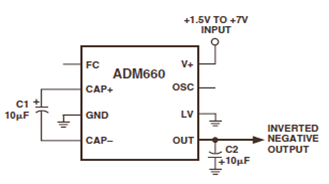
Description: The ADM660 is a charge-pump voltage converter that can either invert the input supply voltage or double it. The schematic below depicts the ADM660 Voltage Inverter Circuit Configuration Diagram. This inverting schematic is ideal for generating a negative rail in single power supply systems. To optimize capacitor size and quiescent current, there is a Frequency Control (FC) input pin instead of the external oscillator (OSC) pin, according to the datasheet. This device is commonly used in applications such as handheld instruments, portable computers, remote data acquisition, and operational amplifier power supplies. For complete information, refer to the ADM660 Datasheet.
The ADM660 is a versatile charge-pump voltage converter capable of performing both voltage inversion and doubling functions. It operates effectively in applications where a negative voltage rail is required, particularly in single-supply systems. The circuit configuration typically consists of a few essential components: the ADM660 IC itself, capacitors for charge storage, and external connections for input and output voltages.
The device's ability to invert or double the input voltage is facilitated by its internal charge pump circuitry, which utilizes capacitors to transfer charge efficiently. The inclusion of a Frequency Control (FC) input pin allows for fine-tuning of the operating frequency, which can enhance performance by optimizing the size of the capacitors used in the circuit while maintaining low quiescent current levels. This is particularly beneficial in battery-operated devices where power efficiency is critical.
The ADM660 is suitable for a wide range of applications, including portable electronics, where space and power constraints are paramount. It is also applicable in remote data acquisition systems, where stable and reliable power supplies are necessary. Furthermore, the device can be utilized to power operational amplifiers that require dual supply voltages.
In designing a circuit with the ADM660, it is essential to follow the recommended guidelines outlined in the datasheet. This includes selecting appropriate capacitor values to achieve the desired voltage conversion and ensuring that the input voltage levels are within the specified range for optimal performance. Overall, the ADM660 provides a compact and efficient solution for voltage conversion needs in various electronic applications.The ADM660 is a charge-pump voltage converter that can be used to either invert the input supply voltage or double it. The schematic below appearsADM660 Voltage Inverter Circuit Configuration Diagram. This inverting schematic is ideal for generating a negative rail in single power supply systems. In order to optimize capacitor size and quiescent c urrent, there is a Frequency Control (FC) input pin instead of the external oscillator (OSC) pin, according to the datasheet. This device used to be applied in applications such Handheld Instruments, Portable Computers, Remote Data Acquisition and Op Amp Power Supplies.
See complete read on thisCharge Pump Voltage Inverter Devicein the ADM660 Datasheet (source: analog. com).
The ADM660 is a versatile charge-pump voltage converter capable of performing both voltage inversion and doubling functions. It operates effectively in applications where a negative voltage rail is required, particularly in single-supply systems. The circuit configuration typically consists of a few essential components: the ADM660 IC itself, capacitors for charge storage, and external connections for input and output voltages.
The device's ability to invert or double the input voltage is facilitated by its internal charge pump circuitry, which utilizes capacitors to transfer charge efficiently. The inclusion of a Frequency Control (FC) input pin allows for fine-tuning of the operating frequency, which can enhance performance by optimizing the size of the capacitors used in the circuit while maintaining low quiescent current levels. This is particularly beneficial in battery-operated devices where power efficiency is critical.
The ADM660 is suitable for a wide range of applications, including portable electronics, where space and power constraints are paramount. It is also applicable in remote data acquisition systems, where stable and reliable power supplies are necessary. Furthermore, the device can be utilized to power operational amplifiers that require dual supply voltages.
In designing a circuit with the ADM660, it is essential to follow the recommended guidelines outlined in the datasheet. This includes selecting appropriate capacitor values to achieve the desired voltage conversion and ensuring that the input voltage levels are within the specified range for optimal performance. Overall, the ADM660 provides a compact and efficient solution for voltage conversion needs in various electronic applications.The ADM660 is a charge-pump voltage converter that can be used to either invert the input supply voltage or double it. The schematic below appearsADM660 Voltage Inverter Circuit Configuration Diagram. This inverting schematic is ideal for generating a negative rail in single power supply systems. In order to optimize capacitor size and quiescent c urrent, there is a Frequency Control (FC) input pin instead of the external oscillator (OSC) pin, according to the datasheet. This device used to be applied in applications such Handheld Instruments, Portable Computers, Remote Data Acquisition and Op Amp Power Supplies.
See complete read on thisCharge Pump Voltage Inverter Devicein the ADM660 Datasheet (source: analog. com).
voltage inverter
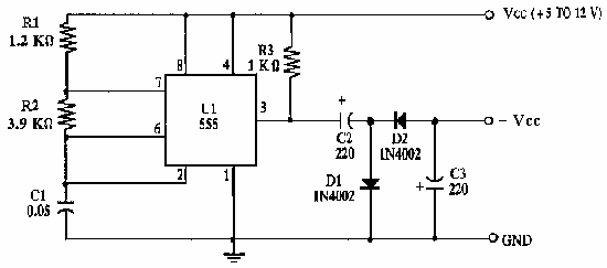
This circuit inverts the polarity of the input. Output is limited to less than 200mA. More: U1 NE555 timer IC R1 1.2k ohm resistor R2 3.9k ohm resistor R3 1k ohm resistor C1 0.05 uF ceramic capacitor C2, C3 220...
6vdc to 12vdc converter circuit
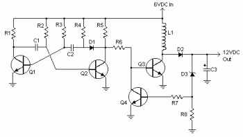
Various values of D3 can be utilized to achieve different output voltages ranging from approximately 0.6V to around 30V. It is important to note that at elevated voltages, the circuit's performance may diminish, potentially resulting in lower current output. Additionally,...
Voltage Converter 6 to 12 Volts -Using TDA 2003
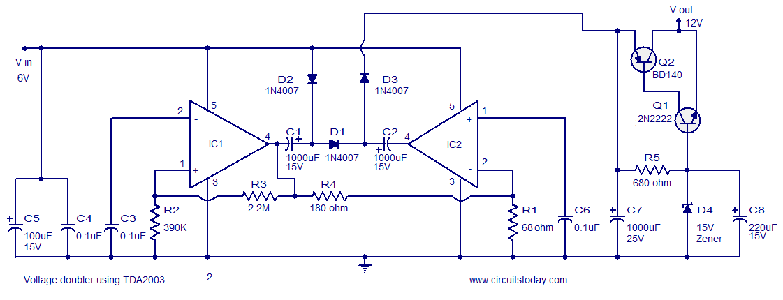
A reliable voltage converter circuit that operates between 6 to 12 volts, utilizing the audio amplifier IC TDA 2003. This voltage doubler circuit can be assembled on a Vero board.
The voltage converter circuit designed with the TDA 2003 audio amplifier...
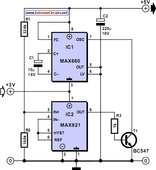
Inductorless 3-5 Volts Converter
By configuring a comparator and a transistor to control the oscillator in a charge pump circuit, it is possible to generate a regulated output of virtually any desired value. Charge pump integrated circuits (ICs) can either invert or double an...
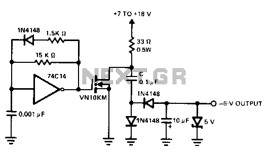
Positive-input-negative-output-charge-pump
A charge pump is a straightforward method for generating a low-power voltage supply of opposite polarity from the main supply. The 74CL4 IC serves as a self-oscillating driver for the MOSFET power switch, producing a pulse width of 6.5 microseconds...
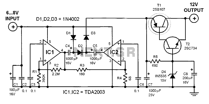
6v to 12v converter
This 6V to 12V converter circuit is made with an IC from SGS with several additional components. The IC is a TDA2003 but it can be replaced with a TDA2002. The cost of building the 6 volts to 12 volts...
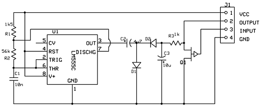
A voltage inverter circuit
Our programmable MP3 player has an interface to an LCD with a HD44780 controller. These are alphanumeric LCDs with one to 4 lines of text and 16 to 40 characters per line. However, these LCDs (and LCDs in general) exist...
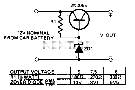
12V to 9 or 6 v converter
This circuit allows transistorized devices, such as radios, cassette players, and other electrical appliances, to operate from a car's electrical supply. The accompanying table provides resistor values and specifies diode types for different voltage levels. If multiple voltage levels are...
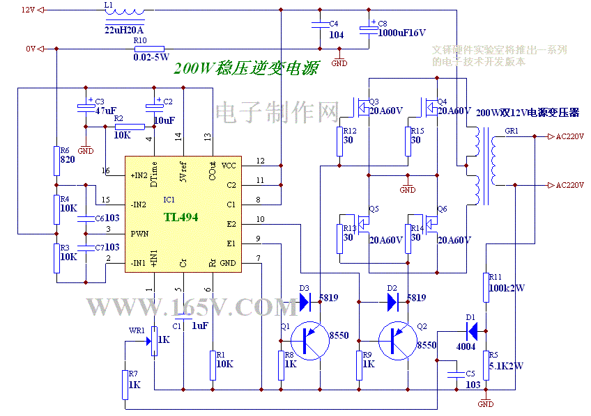
Stabilized voltage inverter 12V-220V 200W
A stabilized voltage inverter that converts 12V to 220V with a power rating of 200W is illustrated in the accompanying diagram. This inverter can utilize an existing dual 12V-200W mains transformer; however, it exhibits low inverter efficiency.
The described stabilized voltage...