


DC/DC boost converter
#DC/DC boost converter
#voltage conversion
#duty cycle
#power electronics
#voltage regulator
#step-up converter
#switching circuit
#energy efficiency
#load resistor
#datasheet specifications
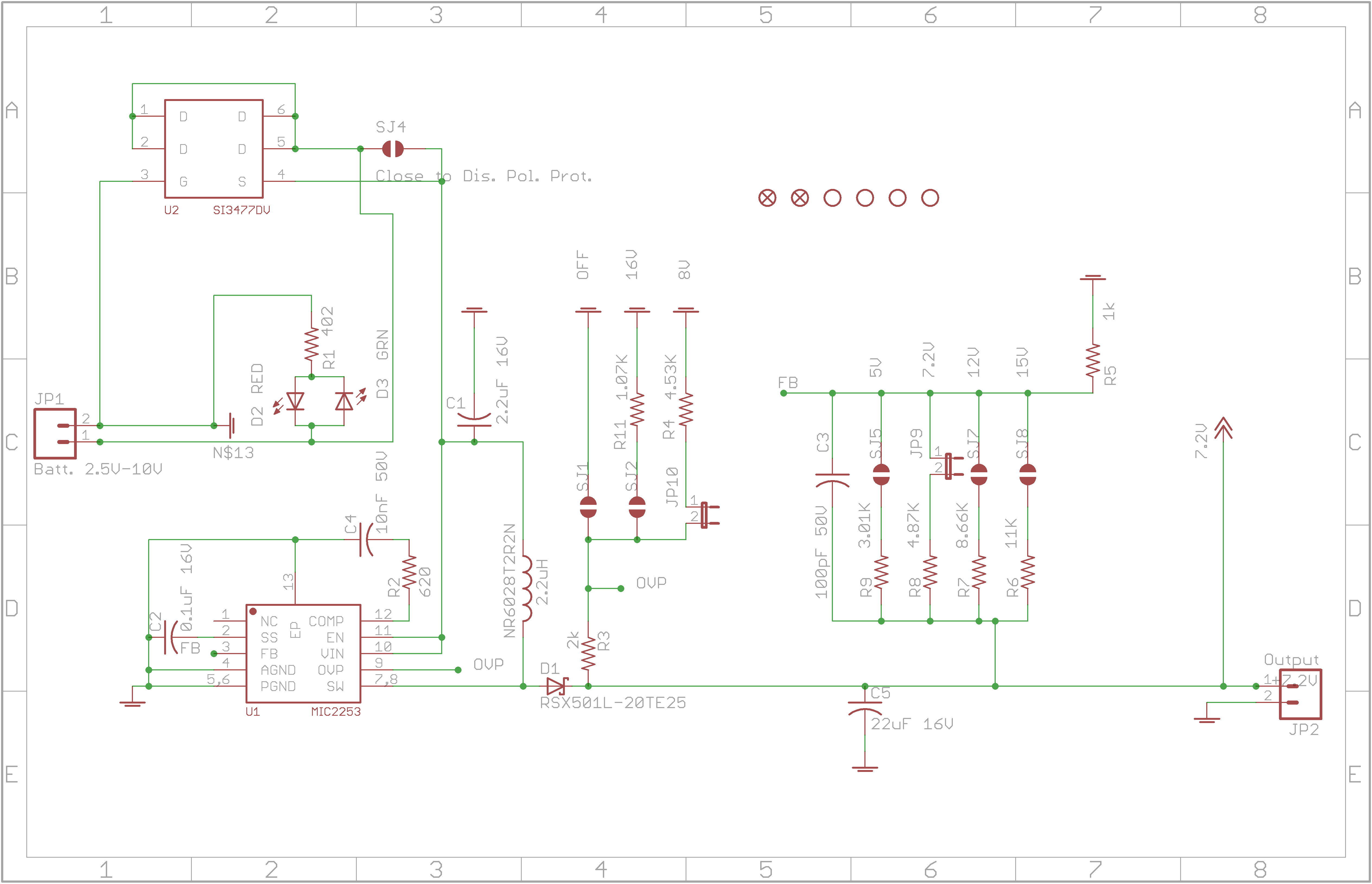
Description: The circuit allows for various combinations of input voltages (Vin) and output voltages (Vout). The current case under debugging involves Vin=3.6V and Vout=7.2V, with a load represented by a 120-ohm resistor. The calculated duty cycle is D=0.5, indicating 50%, which falls within the specified limits of 10% minimum and 90% maximum duty cycle as per the datasheet. All other components, including capacitors, inductors, and resistors, are consistent with the datasheet's application example. The design successfully generates the correct RMS step-up voltage at the output; however, oscilloscope observations reveal damped sinusoidal voltage oscillations occurring periodically, likely initiated by the inductor's switching action. These oscillations are present at nearly every ground point on the board, with peak-to-peak amplitudes reaching 3V. Research indicates that these issues may not be specific to the converter selection but rather related to the PCB layout. Images attached include "original pcb.png," showing the problematic two-layer board with red as the top copper layer and blue as the bottom copper layer, and "current loops.jpg," which illustrates the orange and yellow overlays representing the current paths for charging and discharging the inductor. An article suggested minimizing the area of these current loops, leading to a new layout attempt depicted in "pcb_fix.png." Modifications were made to the original PCB to approach this new layout; however, performance remained unchanged, with persistent noise. Concerns include potential parasitic capacitance from the ground pour, high impedance in the capacitors, and excessive inductance in the traces. Although a shielded inductor was selected, there is uncertainty regarding its magnetic field's interference with signals. After implementing several changes recommended by Olin Lathrop, a significant reduction in oscillation amplitude was observed, with modifications to the original circuit board reducing oscillations to 2V peak-to-peak. Adding additional 22uF ceramic capacitors had minimal impact, while soldering a 22uF ceramic capacitor between the output pins significantly decreased noise to a maximum amplitude of 150mV peak-to-peak without bandwidth limiting on the oscilloscope. Madmanguruman proposed a similar method, suggesting the addition of two capacitors (10uF electrolytic and 100nF ceramic) in parallel at the probe tip to ground, and limiting measurement bandwidth to 20MHz with the probes set to 1x, which also helped reduce noise. Although the results indicate an initial lack of sufficient capacitance at the output, it remains uncertain whether the achieved noise floor is acceptable for a switching converter. Testing under heavier loading conditions, such as with a 30-ohm resistive load, has revealed new anomalous behavior.
The circuit in question is a voltage step-up converter, likely utilizing a switching topology such as a boost converter. The input voltage (Vin) of 3.6V is stepped up to an output voltage (Vout) of 7.2V, suitable for powering devices requiring higher voltage levels. The duty cycle of 50% indicates that the switch within the converter is on for half of the switching period, which is typical for efficient operation within the specified limits.
The presence of damped sinusoidal oscillations on the output suggests issues related to the PCB layout, particularly with the current loops and grounding scheme. In switching power supplies, the layout is critical for minimizing inductive and capacitive coupling, which can lead to oscillations and noise. The two-layer board setup, with distinct copper layers for signal and ground, may not provide sufficient separation or low-impedance paths for return currents, contributing to the observed oscillations.
The modifications attempted, including the addition of capacitors and layout adjustments, indicate a proactive approach to mitigating noise. The use of ceramic capacitors, known for their low equivalent series resistance (ESR) and inductance (ESL), is appropriate; however, the placement and connection to the output pins are crucial for their effectiveness. The significant improvement in noise levels after adding a capacitor directly at the output indicates that local decoupling is vital for stabilizing the voltage and reducing high-frequency noise.
Further investigation into the inductance of traces and the layout of the ground pour is warranted. It may be beneficial to utilize a ground plane for better current return paths and to minimize loop areas, which can help reduce parasitic inductance. Additionally, exploring the use of ferrite beads or common-mode chokes may assist in filtering out high-frequency noise.
In conclusion, while the circuit demonstrates the capability to step up voltage effectively, attention must be directed towards optimizing the PCB layout and component placement to achieve desired performance under varying load conditions. The observations made during testing, particularly under heavier loads, highlight the need for further refinement to ensure stable operation across all expected conditions.Although my circuit allows for different combinations of input voltages (Vin) and output voltages (Vout). The case I am debugging is with Vin=3. 6V and Vout=7. 2V. The Load was a 120 ohm resistor. I calculated the duty cycle D=0. 5 (i. e. 50%). This seems to be within the 10% minimum and 90% maximum duty cycle limits specified in the datasheet.
The ot her components, i. e. caps, inductors, resistors are the same or similar to what the data sheet suggests in its application example. The design appears to give the correct RMS step up voltage on the output, but, after viewing the signal through an oscilloscope I see damped sinusoidal voltage oscillations appearing periodically which seems to be initiated by the switching of the inductor.
I see the same oscillations on almost every ground point on the board. The oscillations on the output are large, that is 3 V peak to peak. After doing a bit of research it seems that my problems are not particular to my choice of converter, but, to problems with my PCB layout (see links below). I`m not sure how to fix my layout to ensure acceptable results. I`ve attached three images. "original pcb. png" contains an image of the board I am having issues with. It is a 2 layer board. Red is the top copper. Blue is bottom copper. "current loops. jpg" shows the prototype board with orange and yellow overlays of the two different current paths used to charge (orange) and discharge (yellow) the inductor.
One of the articles, ( ), suggested that the two current loops should not change in area, thus, I tried to minimize their the change in area in a new layout I started in "pcb_fix. png". I hacked the original PCB so that it was closer to this new layout, but, the performance of the board didn`t change.
It is still noisy! The quality of the hack isn`t as good as shown in "pcb_fix. png", however, it is a fair approximation. I would have expected somewhat of an improvement, but, I didn`t see any. I`m still not sure how to fix this. Maybe the ground pour is causing too much parasitic capacitance Perhaps the caps have too much impedance (ESR or ESL) I don`t think so, because they are all ceramic multilayer and have the values and dielectric material requested by the datasheet, i. e. X5R. Perhaps my traces might have too much inductance. I chose a shielded inductor, but, is it possible that its magnetic field is interfering with my signals Upon implementing several of the changes suggested by Olin Lathrop, a large decrease in oscillation amplitude was observed.
Hacking the original cicuit board to approximate the new layout helped somewhat by bringing down the oscillations to 2V peak to peak: The addition of additional input 22uF ceramic capacitors made only a negligible difference. However, the overwhelming improvement came from simply soldering a 22uF ceramic cap between the output pins and measuring the signal across the cap.
This brought the noise maximum amplitude to 150mV peak to peak without any bandwidth limiting of the scope! Madmanguruman suggested a similar approach, with the exception that he suggested altering the probe tip instead of the circuit.
He suggested putting two caps between ground and the tip: one 10uF electrolytic and one 100nF ceramic (in parallel I assumed). In addition, he suggested limiting the bandwidth of the measurement to 20Mhz and putting the probes on 1x.
This seemed to have a noise attenuating effect as well in about the same magnitude. I guess I can conclude that there was originally insufficient capacitance at the output. I`m not sure if this is a acceptably low noise floor or even a typical noise amplitude for a switching converter, but, it is a massive improvement. This was encouraging so I went on to test the robustness of the circuit under more significant loading.
Unfortunately, under heavier loading the circuit is producing some new weird behaviour. I tested the circuit with a 30 ohm resistive load. Alth
The circuit in question is a voltage step-up converter, likely utilizing a switching topology such as a boost converter. The input voltage (Vin) of 3.6V is stepped up to an output voltage (Vout) of 7.2V, suitable for powering devices requiring higher voltage levels. The duty cycle of 50% indicates that the switch within the converter is on for half of the switching period, which is typical for efficient operation within the specified limits.
The presence of damped sinusoidal oscillations on the output suggests issues related to the PCB layout, particularly with the current loops and grounding scheme. In switching power supplies, the layout is critical for minimizing inductive and capacitive coupling, which can lead to oscillations and noise. The two-layer board setup, with distinct copper layers for signal and ground, may not provide sufficient separation or low-impedance paths for return currents, contributing to the observed oscillations.
The modifications attempted, including the addition of capacitors and layout adjustments, indicate a proactive approach to mitigating noise. The use of ceramic capacitors, known for their low equivalent series resistance (ESR) and inductance (ESL), is appropriate; however, the placement and connection to the output pins are crucial for their effectiveness. The significant improvement in noise levels after adding a capacitor directly at the output indicates that local decoupling is vital for stabilizing the voltage and reducing high-frequency noise.
Further investigation into the inductance of traces and the layout of the ground pour is warranted. It may be beneficial to utilize a ground plane for better current return paths and to minimize loop areas, which can help reduce parasitic inductance. Additionally, exploring the use of ferrite beads or common-mode chokes may assist in filtering out high-frequency noise.
In conclusion, while the circuit demonstrates the capability to step up voltage effectively, attention must be directed towards optimizing the PCB layout and component placement to achieve desired performance under varying load conditions. The observations made during testing, particularly under heavier loads, highlight the need for further refinement to ensure stable operation across all expected conditions.Although my circuit allows for different combinations of input voltages (Vin) and output voltages (Vout). The case I am debugging is with Vin=3. 6V and Vout=7. 2V. The Load was a 120 ohm resistor. I calculated the duty cycle D=0. 5 (i. e. 50%). This seems to be within the 10% minimum and 90% maximum duty cycle limits specified in the datasheet.
The ot her components, i. e. caps, inductors, resistors are the same or similar to what the data sheet suggests in its application example. The design appears to give the correct RMS step up voltage on the output, but, after viewing the signal through an oscilloscope I see damped sinusoidal voltage oscillations appearing periodically which seems to be initiated by the switching of the inductor.
I see the same oscillations on almost every ground point on the board. The oscillations on the output are large, that is 3 V peak to peak. After doing a bit of research it seems that my problems are not particular to my choice of converter, but, to problems with my PCB layout (see links below). I`m not sure how to fix my layout to ensure acceptable results. I`ve attached three images. "original pcb. png" contains an image of the board I am having issues with. It is a 2 layer board. Red is the top copper. Blue is bottom copper. "current loops. jpg" shows the prototype board with orange and yellow overlays of the two different current paths used to charge (orange) and discharge (yellow) the inductor.
One of the articles, ( ), suggested that the two current loops should not change in area, thus, I tried to minimize their the change in area in a new layout I started in "pcb_fix. png". I hacked the original PCB so that it was closer to this new layout, but, the performance of the board didn`t change.
It is still noisy! The quality of the hack isn`t as good as shown in "pcb_fix. png", however, it is a fair approximation. I would have expected somewhat of an improvement, but, I didn`t see any. I`m still not sure how to fix this. Maybe the ground pour is causing too much parasitic capacitance Perhaps the caps have too much impedance (ESR or ESL) I don`t think so, because they are all ceramic multilayer and have the values and dielectric material requested by the datasheet, i. e. X5R. Perhaps my traces might have too much inductance. I chose a shielded inductor, but, is it possible that its magnetic field is interfering with my signals Upon implementing several of the changes suggested by Olin Lathrop, a large decrease in oscillation amplitude was observed.
Hacking the original cicuit board to approximate the new layout helped somewhat by bringing down the oscillations to 2V peak to peak: The addition of additional input 22uF ceramic capacitors made only a negligible difference. However, the overwhelming improvement came from simply soldering a 22uF ceramic cap between the output pins and measuring the signal across the cap.
This brought the noise maximum amplitude to 150mV peak to peak without any bandwidth limiting of the scope! Madmanguruman suggested a similar approach, with the exception that he suggested altering the probe tip instead of the circuit.
He suggested putting two caps between ground and the tip: one 10uF electrolytic and one 100nF ceramic (in parallel I assumed). In addition, he suggested limiting the bandwidth of the measurement to 20Mhz and putting the probes on 1x.
This seemed to have a noise attenuating effect as well in about the same magnitude. I guess I can conclude that there was originally insufficient capacitance at the output. I`m not sure if this is a acceptably low noise floor or even a typical noise amplitude for a switching converter, but, it is a massive improvement. This was encouraging so I went on to test the robustness of the circuit under more significant loading.
Unfortunately, under heavier loading the circuit is producing some new weird behaviour. I tested the circuit with a 30 ohm resistive load. Alth
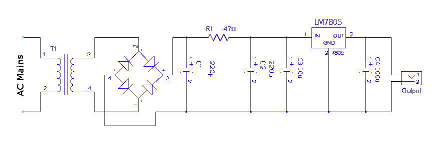
building regulated 5v dc power supply
A regulated 5-volt DC supply is essential for powering microcontroller and TTL-based circuits. The output of most wall adapters is often too rippled and impure for use in digital circuits. An inexpensive power supply can be constructed using discrete components...
Thrifty Voltage Regulator
One of the drawbacks of a three-pin voltage regulator is that the input voltage needs to be 2.5 to 3 V higher than the output voltage. This makes these integrated regulators unsuitable for battery power supplies. For instance, if the...
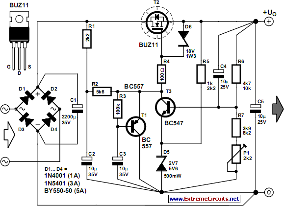
Stable Filament Power Supply Circuit
The circuit diagram illustrates a voltage regulator designed from discrete components to meet specific voltage requirements. It provides two sets of component values for output voltages of 6.3 V (upper) and 12.6 V (lower). The components used include BC547 and...
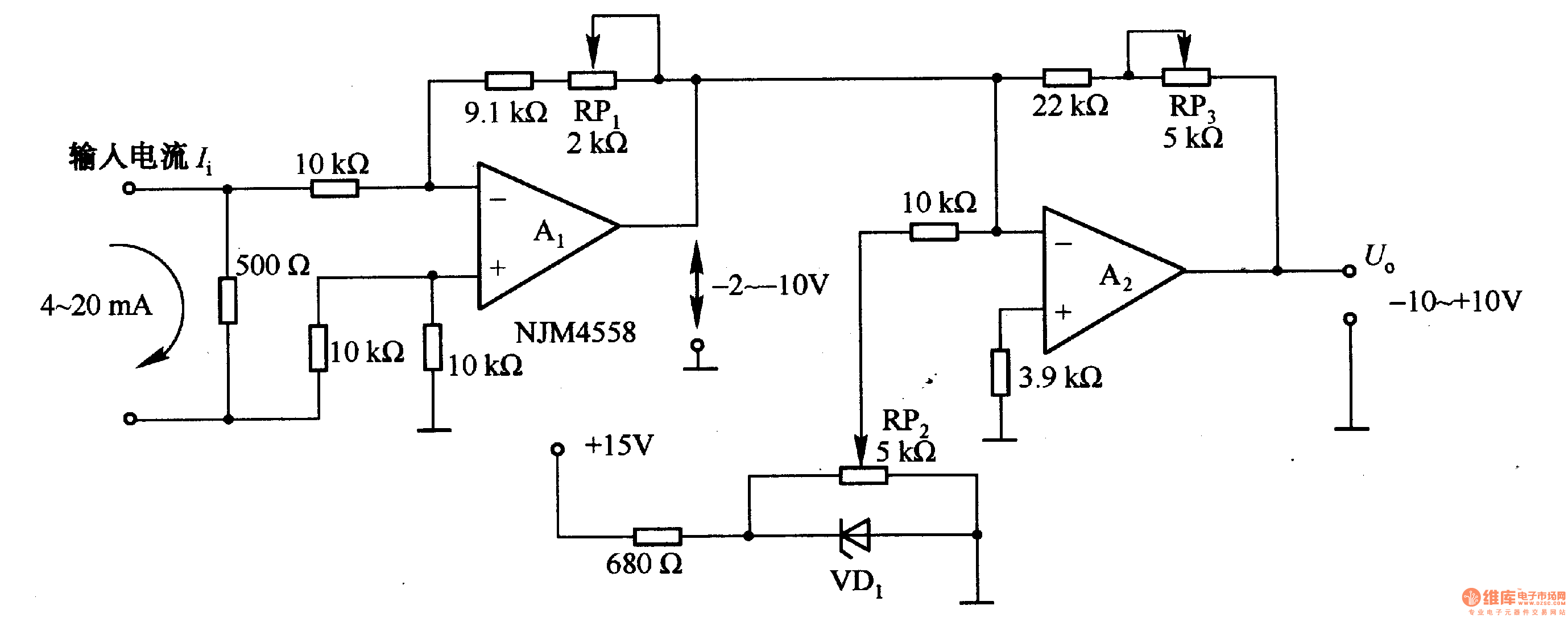
voltage conversion circuit composed of NJM4558
Figure 1-42 (a) is a voltage/current conversion circuit that converts a 0-10V input voltage into a 4-20mA output current. Adjusting resistor RP2 can set the input voltage (Ui) to 0V, resulting in an output current (I) of 20mA; similarly, setting...
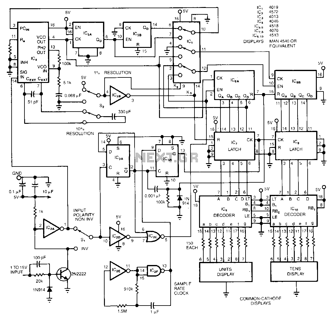
Duty-cycle-monitor
The circuit monitors and displays a digital signal's duty cycle with an accuracy of ±1%. By using switch S2, users can select a frequency range of either 250 Hz to 2.5 kHz with ±1% accuracy or 2 kHz to 50...
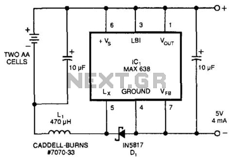
Common Hot-Lead Regulator
This circuit derives 5 V DC from 2 AA cells, even at their end-life voltages of 1.05 V, and is approximately 80% efficient, providing 5 V at 4 mA from 2.1 V at 11 mA. IC1 is manufactured by Maxim...
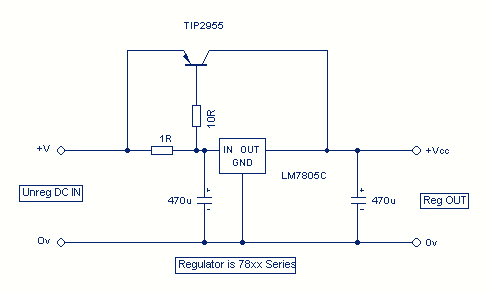
Increasing Regulator Current
Although the 78xx series of voltage regulators are available with different current outputs, you can boost the available current output with this circuit. A power transistor is used to supply extra current to the load, maintaining a constant voltage. Currents...
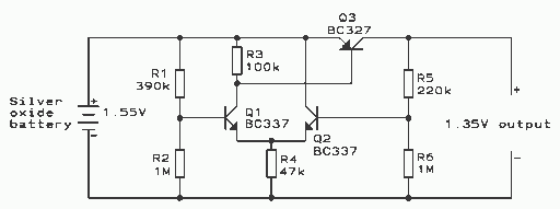
Voltage Regulator
This regulator is suitable for devices that need up to 1mA. For higher output current, the resistors would have to be scaled down in reverse proportion to the peak current expected. With the resistor values shown, the regulator draws a...
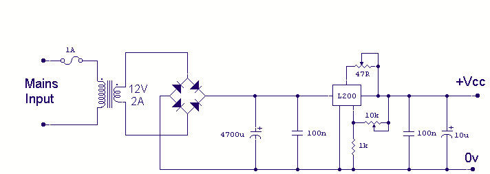
Variable Power Supply
Using the versatile L200 voltage regulator, this power supply has independent voltage and current limits. The mains transformer has a 12-volt, 2 amp rated secondary, the primary winding should equal the electricity supply in your country, which is 240V here...