


Low Loss Step Down Converter
#step down converter
#voltage regulation
#solar power
#battery
#low loss
#5V output
#24V input
#energy efficiency
#power management
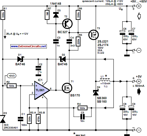
Description: This circuit was designed to provide a 5 V output from a 24 V battery of a solar-powered generator. While solar power is essentially free, it is crucial to avoid waste, especially in small installations; if the battery depletes at midnight, there will be a long wait for the sun to rise again. The primary requirement was to create an efficient step-down converter to power low-voltage equipment. The final design accepts a wide input voltage range from 9 to 60 V, with an output current of 500 mA. The efficiency is notably high, as even with a load of 1 mA, the design outperforms a standard linear regulator. The low quiescent current (200 µA) also contributes to reducing losses. Some specified components, particularly the power MOSFET, may not be the most economical, but they have been intentionally chosen for their efficiency. When power is applied to the circuit, a reference voltage is generated across R2. Diode D1 connects this to the supply (pin 7) of IC1 to provide power during start-up. Once the circuit begins switching and the output voltage rises to 5 V, D2 becomes forward biased, powering the IC from the output. Diode D1 then becomes reverse biased, reducing current through R1. Initially, when the circuit is powered, the voltage on pin 2 of IC1 is below the reference voltage on pin 3, resulting in a high level on output pin 6. This activates the low power MOSFET T1, which in turn switches the power MOSFET T3 via R5 and the speed-up capacitor C4, causing the output voltage to rise. As the output approaches 5 V, the voltage fed back to the inverting input of IC1 becomes positive relative to the non-inverting input (reference), causing the output of IC1 to switch low. T1 and T3 then turn off, and C3 transfers this negative-going edge to the base of T2, which conducts and effectively shorts out the gate capacitance of T3, enhancing its switch-off time. The switching frequency is not fixed but varies with load current; without load, the circuit oscillates at approximately 40 Hz, while at 500 mA, it operates around 5 kHz. This variable clock rate necessitates a relatively high output inductor L1 value of 100 mH. The coil should be wound on ferrite core material with a high AL value to minimize the number of turns and achieve the lowest resistance. Off-the-shelf coils of this value often exceed 1Ω resistance, making them suitable only for output load currents below 100 mA. The output voltage is set by the voltage divider ratio formed by R4 and R3, which can be adjusted for different output voltage requirements. The output voltage must remain at least 1 V below the input voltage, with a minimum output of 4 V due to the supply to IC1. Maximum efficiency of around 90% was achieved with input voltages between 9 and 15 V while supplying currents greater than 5 mA; even at 30 V input, the circuit maintained around 80% efficiency. For lower input voltages, efficiency gains can be realized by replacing D4 with a similar device having a lower reverse breakdown voltage rating, as these typically exhibit a smaller forward voltage drop, thereby reducing diode losses at high currents. At higher input voltage levels, increasing the value of resistor R1 proportionally can further decrease the quiescent current.
The circuit employs a buck converter topology, which is adept at stepping down voltage efficiently. The use of a high-quality power MOSFET ensures minimal conduction losses, while the feedback mechanism involving IC1 maintains the output voltage stability. The switching action of T1 and T3 is crucial for energy transfer from the input to the output, and the inclusion of capacitors C3 and C4 aids in managing transient responses and improving overall efficiency. The design's adaptability to various input voltages makes it suitable for diverse applications in solar energy systems, particularly where low power consumption is essential. The careful selection of components, particularly in terms of their electrical characteristics, underpins the circuit's performance and operational longevity.This circuit arose from the need of the author to provide a 5 V output from the 24 V battery of a solar powered generator. Although solar power is essentially free it is important not to be wasteful especially for small installations; if the battery runs flat at midnight you`ve got a long wait before the sun comes up again.
The basic requirement w as to make an efficient step-down converter to power low voltage equipment; the final design shown here accepts a wide input voltage from 9 to 60 V with an output current of 500 mA. The efficiency is very good even with a load of 1 mA the design is still better than a standard linear regulator.
The low quiescent current (200 µA) also plays a part in reducing losses. Some of the components specified (particularly the power MOSFET) are not the most economical on the market but they have been deliberately selected with efficiency in mind. When power is applied to the circuit a reference voltage is produced on one side of R2. D1 connects this to the supply (pin 7) of IC1 to provide power at start-up. Once the circuit begins switching and the output voltage rises to 5 V, D2 becomes forward biased and powers the IC from the output.
Diode D1 becomes reverse biased reducing current hrough R1. When the circuit is first powered up the voltage on pin 2 of IC1 is below the reference voltage on pin 3, this produces a high level on output pin 6. The low power MOSFET T1 is switched on which in turn switches the power MOSFET T3 via R5 and the speed-up capacitor C4, the output voltage starts to rise.
When the output approaches 5 V the voltage fed back to the inverting input of IC1 becomes positive with respect to the non inverting input (reference) and switches the output of IC1 low. T1 and T3 now switch off and C3 transfers this negative going edge to the base of T2 which conducts and effectively shorts out the gate capacitance of T3 thereby improving its switch off time.
The switching frequency is not governed by a fixed clock signal but instead by the load current; with no load attached the circuit oscillates at about 40 Hz while at 500 mA it runs at approximately 5 kHz. The variable clock rate dictates that the output inductor L1 needs to have the relatively high value of 100 mH.
The coil can be wound on ferrite core material with a high AL value to allow the smallest number of turns and produce the lowest possible resistance. Ready-made coils of this value often have a resistance greater than 1R and these would only be suitable for an output load current of less than 100 mA.
The voltage divider ratio formed by R4 and R3 sets the output voltage and these values can be changed if a different output voltage is required. The output voltage must be a minimum of 1 V below the input voltage and the output has a minimum value of 4 V because of the supply to IC1.
A maximum efficiency of around 90 % was achieved with this circuit using an input voltage between 9 and 15 V and supplying a current greater than 5 mA, even with an input voltage of 30 V the circuit efficiency was around 80 %. If the circuit is used with a relatively low input voltage efficiency gains can be made by replacing D4 with a similar device with a lower reverse breakdown voltage rating, these devices tend to have a smaller forward voltage drop which reduces losses in the diode at high currents.
At higher input voltage levels the value of resistor R1 can be increased proportionally to reduce the quiescent current even further.
The circuit employs a buck converter topology, which is adept at stepping down voltage efficiently. The use of a high-quality power MOSFET ensures minimal conduction losses, while the feedback mechanism involving IC1 maintains the output voltage stability. The switching action of T1 and T3 is crucial for energy transfer from the input to the output, and the inclusion of capacitors C3 and C4 aids in managing transient responses and improving overall efficiency. The design's adaptability to various input voltages makes it suitable for diverse applications in solar energy systems, particularly where low power consumption is essential. The careful selection of components, particularly in terms of their electrical characteristics, underpins the circuit's performance and operational longevity.This circuit arose from the need of the author to provide a 5 V output from the 24 V battery of a solar powered generator. Although solar power is essentially free it is important not to be wasteful especially for small installations; if the battery runs flat at midnight you`ve got a long wait before the sun comes up again.
The basic requirement w as to make an efficient step-down converter to power low voltage equipment; the final design shown here accepts a wide input voltage from 9 to 60 V with an output current of 500 mA. The efficiency is very good even with a load of 1 mA the design is still better than a standard linear regulator.
The low quiescent current (200 µA) also plays a part in reducing losses. Some of the components specified (particularly the power MOSFET) are not the most economical on the market but they have been deliberately selected with efficiency in mind. When power is applied to the circuit a reference voltage is produced on one side of R2. D1 connects this to the supply (pin 7) of IC1 to provide power at start-up. Once the circuit begins switching and the output voltage rises to 5 V, D2 becomes forward biased and powers the IC from the output.
Diode D1 becomes reverse biased reducing current hrough R1. When the circuit is first powered up the voltage on pin 2 of IC1 is below the reference voltage on pin 3, this produces a high level on output pin 6. The low power MOSFET T1 is switched on which in turn switches the power MOSFET T3 via R5 and the speed-up capacitor C4, the output voltage starts to rise.
When the output approaches 5 V the voltage fed back to the inverting input of IC1 becomes positive with respect to the non inverting input (reference) and switches the output of IC1 low. T1 and T3 now switch off and C3 transfers this negative going edge to the base of T2 which conducts and effectively shorts out the gate capacitance of T3 thereby improving its switch off time.
The switching frequency is not governed by a fixed clock signal but instead by the load current; with no load attached the circuit oscillates at about 40 Hz while at 500 mA it runs at approximately 5 kHz. The variable clock rate dictates that the output inductor L1 needs to have the relatively high value of 100 mH.
The coil can be wound on ferrite core material with a high AL value to allow the smallest number of turns and produce the lowest possible resistance. Ready-made coils of this value often have a resistance greater than 1R and these would only be suitable for an output load current of less than 100 mA.
The voltage divider ratio formed by R4 and R3 sets the output voltage and these values can be changed if a different output voltage is required. The output voltage must be a minimum of 1 V below the input voltage and the output has a minimum value of 4 V because of the supply to IC1.
A maximum efficiency of around 90 % was achieved with this circuit using an input voltage between 9 and 15 V and supplying a current greater than 5 mA, even with an input voltage of 30 V the circuit efficiency was around 80 %. If the circuit is used with a relatively low input voltage efficiency gains can be made by replacing D4 with a similar device with a lower reverse breakdown voltage rating, these devices tend to have a smaller forward voltage drop which reduces losses in the diode at high currents.
At higher input voltage levels the value of resistor R1 can be increased proportionally to reduce the quiescent current even further.
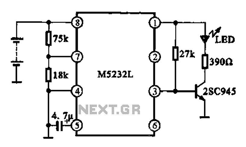
Battery voltage indication circuit
A battery voltage indication circuit that changes the status display. When the battery voltage is normal, an additional transistor drives an LED, which remains off. However, if the battery voltage falls below a critical threshold, the LED begins to flash,...
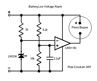
Precision Receiver Battery Low Voltage Alarms
Flying hand launch gliders necessitate the use of small-capacity receiver NiCad battery packs. While these lightweight packs are advantageous, they have the significant drawback of quickly depleting. Although careful timing of flights can be employed, it often results in either...
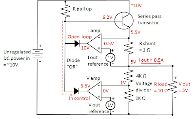
how does power supply regulate its
Most power supplies regulate either their output voltage or current at a constant level, depending on the load resistance relative to the power supply's output voltage and current settings. This can be summarized as follows: To accomplish this, most power...
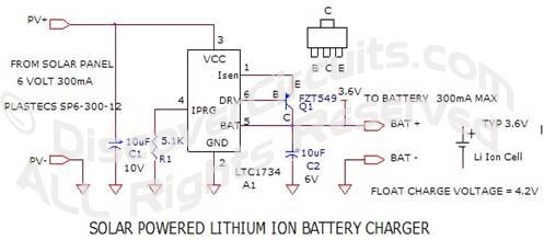
solar circuits
The controller for the Hybrid Power Plant (HPP) is represented in a block diagram format. It consists of 440 Wp photovoltaic modules, a 1 kW wind turbine, and a 5 kW diesel engine as a backup power source. The HPP...

psu
The Chameleon II Power Supply Circuits convert the raw input supply into stable voltage outputs necessary for the Chameleon interfaces. The outputs provided are +5V, +12V, and -12V.
The Chameleon II Power Supply Circuits are designed to ensure reliable operation of...
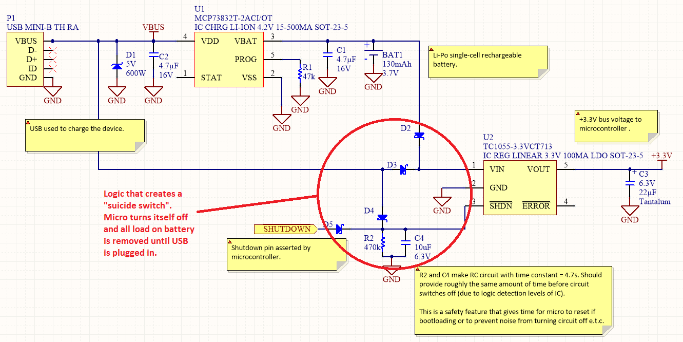
Power Management
Overview Disabling Sections of a Circuit The "Suicide Switch" Overview Power management is a significant design consideration for battery-powered devices.
Power management is a crucial aspect of circuit design, particularly in battery-powered applications where energy efficiency directly impacts the operational lifespan...
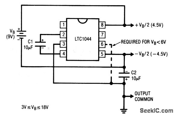
Micropower battery splitter
This circuit generates symmetrical ±output voltages, each equal to one-half of the input voltage (for example, a single 9-V battery). The output voltages are referenced to pin 3, which serves as the output common. The circuit is compatible with different...
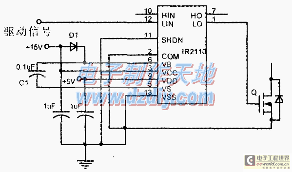
Design and making of the stabilized voltage supply of switch
Under the loading condition of the resistance, the output voltage (Uo) variable range is from 30V to 36V, with a maximum output current (Imax) of 2A. When the input voltage (U2) changes from 15V to 21V, the voltage regulation factor...
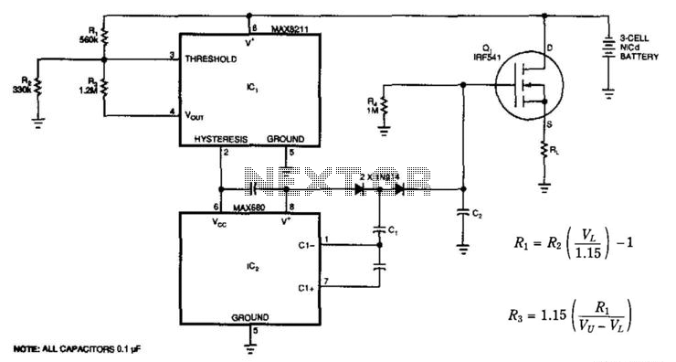
Battery-Saving Disconnect Switch
At a predetermined level of declining terminal voltage, the circuit disconnects the battery from the load and halts potentially destructive battery discharge. Q1, a high-side, floating-source MOSFET, acts as the switch. The overall circuit draws about 500 µA when the...