


Low Voltage 2mhz Step-up Dc/dc Converter
#DC/DC converter
#step-up
#boost converter
#USB power
#voltage regulation
#switching
#5V output
#500mA
#low voltage
#AAT1275
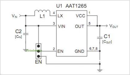
Description: The AAT1275 evaluation board serves as a platform for testing and evaluating the AAT1275 switching boost converter equipped with a USB power switch. This evaluation board showcases the recommended size and placement of external components to achieve 5V output voltages and support output load currents of up to 500mA, facilitating USB VBUS operation from an input supply as low as 2.7V. The external components are chosen for their compact size, making them suitable for portable applications, while the layout has been optimized for high efficiency and low output noise using the TSOPJW-12 package. The design operates within an input voltage range of 2.7V to 5V. This document outlines the operation and testing of the AAT1275 evaluation board. By modifying the resistor divider network (R2, R3), different output voltages can be achieved. The load switch current limit level at OUT2 is determined by the value of RSET (R4) as indicated in Table 1. When the load current at the OUT2 pin exceeds the current limit, the AAT1275 shuts down to reduce power dissipation and component stress during overload and short circuit conditions.
The AAT1275 evaluation board is designed to facilitate the assessment of the AAT1275 switching boost converter, which is particularly valuable in applications requiring efficient power conversion from low voltage sources. The board's compact design is optimized for portable applications, making it suitable for integration into various consumer electronics.
The evaluation board operates effectively within an input voltage range of 2.7V to 5V, allowing it to accommodate a variety of power sources. A key feature of this design is its ability to provide a stable 5V output voltage capable of delivering up to 500mA of load current, which is essential for USB VBUS operation. The selection of external components is critical; they are chosen not only for their size but also for their performance characteristics, ensuring that the converter operates with high efficiency and minimal output noise.
The TSOPJW-12 package encapsulates the AAT1275, providing a compact footprint while ensuring thermal performance is maintained. The layout of the evaluation board is meticulously designed to minimize parasitic inductance and resistance, which contributes to the overall efficiency of the boost converter.
The evaluation board includes a resistor divider network (R2, R3) that allows for the adjustment of output voltage levels, enabling flexibility in various applications. Additionally, the load switch current limit at OUT2 is set by RSET (R4), providing a safeguard against excessive current draw. This feature is particularly important for protecting the circuit from potential damage due to overload or short circuit conditions. When the current at OUT2 exceeds the predefined limit, the AAT1275 automatically enters a shutdown mode, effectively minimizing power dissipation and reducing stress on the components.
Overall, the AAT1275 evaluation board is a robust platform for evaluating the performance of the AAT1275 boost converter, offering essential features and flexibility for a wide range of applications in portable electronics.The AAT1275 evaluation board provides a platform for test and evaluation of the AAT1275 switching boost converter with USB Power Switch The evaluation board demonstrates suggested size and placement of external components to achieve 5V output voltages and up to 500mA output load current to support USB VBUS operation from an input supply as low as 2. 7V. The external components are selected for small size to suit portable applications while the layout has been optimized to achieve high efficiency and low output noise with the TSOPJW-12 package. The design operates across an input voltage range from 2. 7 to 5V. This document provides details on the operation and test of the AAT1275 Evaluation Board. Modification of the resistor divider network (R2, R3) allows different output voltages. The load Switch current limit level at OUT2 is determined by RSET (R4) value (see Table 1). When the OUT2 pin load current has exceeded current limit level the AAT1275 shuts down to minimize the power dissipation and component stresses under over load and short circuit conditions.
The AAT1275 evaluation board is designed to facilitate the assessment of the AAT1275 switching boost converter, which is particularly valuable in applications requiring efficient power conversion from low voltage sources. The board's compact design is optimized for portable applications, making it suitable for integration into various consumer electronics.
The evaluation board operates effectively within an input voltage range of 2.7V to 5V, allowing it to accommodate a variety of power sources. A key feature of this design is its ability to provide a stable 5V output voltage capable of delivering up to 500mA of load current, which is essential for USB VBUS operation. The selection of external components is critical; they are chosen not only for their size but also for their performance characteristics, ensuring that the converter operates with high efficiency and minimal output noise.
The TSOPJW-12 package encapsulates the AAT1275, providing a compact footprint while ensuring thermal performance is maintained. The layout of the evaluation board is meticulously designed to minimize parasitic inductance and resistance, which contributes to the overall efficiency of the boost converter.
The evaluation board includes a resistor divider network (R2, R3) that allows for the adjustment of output voltage levels, enabling flexibility in various applications. Additionally, the load switch current limit at OUT2 is set by RSET (R4), providing a safeguard against excessive current draw. This feature is particularly important for protecting the circuit from potential damage due to overload or short circuit conditions. When the current at OUT2 exceeds the predefined limit, the AAT1275 automatically enters a shutdown mode, effectively minimizing power dissipation and reducing stress on the components.
Overall, the AAT1275 evaluation board is a robust platform for evaluating the performance of the AAT1275 boost converter, offering essential features and flexibility for a wide range of applications in portable electronics.The AAT1275 evaluation board provides a platform for test and evaluation of the AAT1275 switching boost converter with USB Power Switch The evaluation board demonstrates suggested size and placement of external components to achieve 5V output voltages and up to 500mA output load current to support USB VBUS operation from an input supply as low as 2. 7V. The external components are selected for small size to suit portable applications while the layout has been optimized to achieve high efficiency and low output noise with the TSOPJW-12 package. The design operates across an input voltage range from 2. 7 to 5V. This document provides details on the operation and test of the AAT1275 Evaluation Board. Modification of the resistor divider network (R2, R3) allows different output voltages. The load Switch current limit level at OUT2 is determined by RSET (R4) value (see Table 1). When the OUT2 pin load current has exceeded current limit level the AAT1275 shuts down to minimize the power dissipation and component stresses under over load and short circuit conditions.
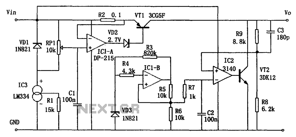
High-performance power supply LM334
The circuit functions as a switching power supply designed to operate alongside a linear regulated power supply. Key characteristics include high efficiency and low dropout voltage. It effectively filters out high-frequency ripple voltage and manages instantaneous voltage variations, making it...
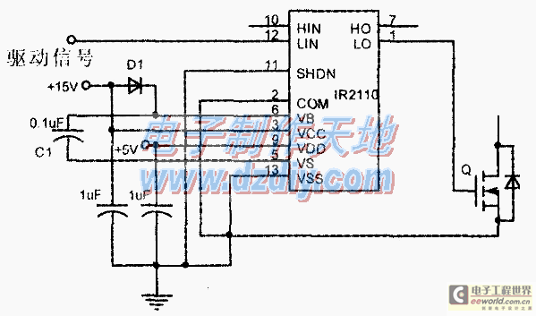
Design and making of the stabilized voltage supply of switch
Under the loading condition of the resistance, the output voltage (Uo) variable range is from 30V to 36V, with a maximum output current (Imax) of 2A. When the input voltage (U2) changes from 15V to 21V, the voltage regulation factor...
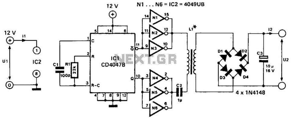
Dc/Dc Converter Circuit
This low-power converter supplies approximately 100 mW of DC power to a load and is useful for isolating or deriving DC voltages. It operates at a frequency of around 200 kHz. The inductor is wound on a 22-mm diameter, 13-mm...

psu
The Chameleon II Power Supply Circuits convert the raw input supply into stable voltage outputs necessary for the Chameleon interfaces. The outputs provided are +5V, +12V, and -12V.
The Chameleon II Power Supply Circuits are designed to ensure reliable operation of...
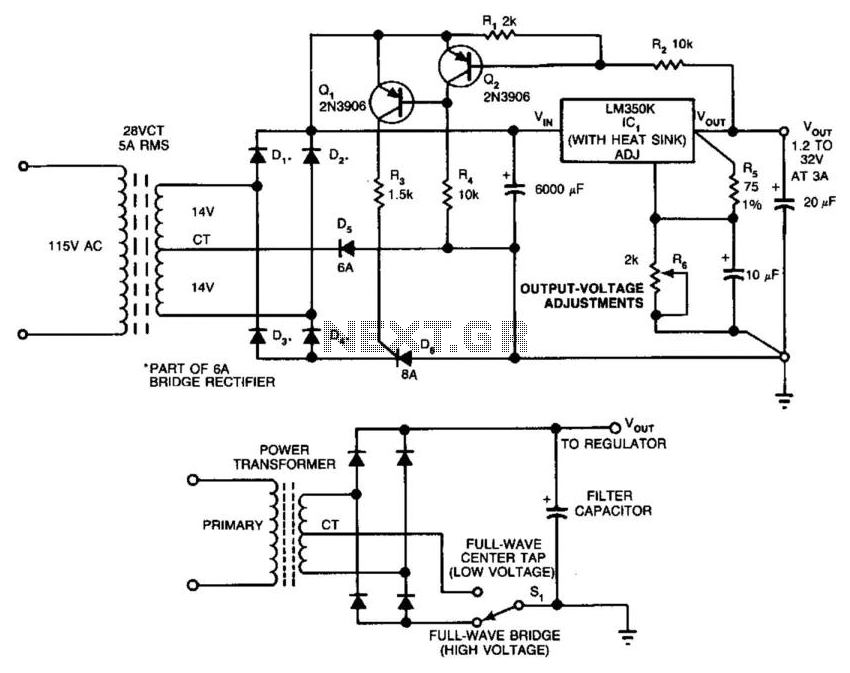
Switching Improves Regulator Efficiency
In this circuit, a full-wave bridge is switched to a full-wave center tap to reduce regulator dissipation. SCR D6 switches between configurations. When D6 is off, the circuit is an FWCT rectifier using D1, D2, and D5. It applies 17...
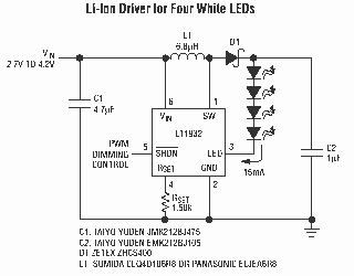
DC/DC LED Driver in ThinSOT
The LT1932 is a fixed frequency step-up DC/DC converter designed to operate as a constant-current source. Because it directly regulates output current, the LT1932 is ideal for driving light emitting diodes (LEDs) whose light intensity is proportional to the current...
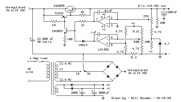
Variable Voltage and Current Power Supply circuit
An alternative approach to utilizing operational amplifiers (op-amps) for power supply regulation is presented. This method necessitates an additional winding on the power transformer to provide the op-amps with a bipolar voltage of +/- 8 volts. The negative voltage generated...
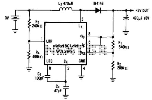
3V Battery To 5V Dc/Dc Converter
A common power supply requirement involves converting a 2.4- or 3-V battery voltage to a 5-V logic supply. This circuit converts 3 V to 5 V at 40 mA with 85% efficiency. When the IC (pin 6) is driven low,...
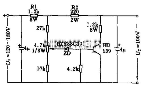
100v / 10ma regulator circuit
The circuit features no-load and short circuit protection mechanisms. To accommodate short circuit conditions, it is necessary to increase resistors R1 and R2 to allow for power dissipation; for example, R1 can be set to 1.2kΩ with a power rating...