


Precision Full-Wave Ac/Dc Converter
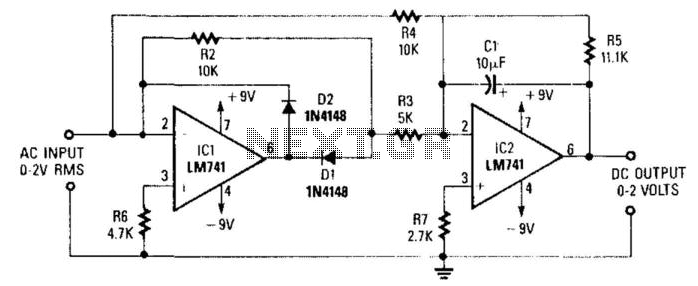
Description: A DC level is generated that corresponds to the AC input RMS value (for a sine wave). The gain of the integrated circuit (IC) is set to a factor of 2 to 1.11. This factor represents the average-to-RMS conversion ratio. IC1 and IC2 function as a full-wave rectifier circuit, utilizing diodes D1 and D2.
The described circuit is designed to convert an alternating current (AC) signal into a direct current (DC) level that accurately reflects the root mean square (RMS) value of the input signal, particularly when the input is a sine wave. The gain setting of the integrated circuit (IC) is crucial for ensuring that the output voltage level is proportional to the RMS value of the input signal. The specified gain range of 2 to 1.11 indicates that the circuit can be calibrated to provide an output that is either twice or slightly more than the average value of the input AC signal, depending on the specific application requirements.
The full-wave rectifier configuration, implemented with IC1 and IC2 along with diodes D1 and D2, allows for the effective conversion of both halves of the AC waveform into a unidirectional current. This configuration enhances the efficiency of the rectification process by minimizing the ripple voltage in the output, which is particularly important for applications that require a stable DC level for further processing or measurement.
In this setup, diodes D1 and D2 are oriented to conduct during opposite halves of the AC cycle, ensuring that the output voltage remains positive regardless of the input polarity. The choice of diodes is critical; they must have a suitable forward voltage drop and recovery time to minimize losses and ensure quick response times for varying input frequencies.
The output from the rectification stage is then filtered to smooth out any remaining ripple, typically using capacitors and possibly inductors, before being fed into subsequent stages of the circuit that may include additional amplification or analog-to-digital conversion, depending on the intended application. Overall, this circuit design is integral for applications requiring precise measurement or control of AC signals in a DC format. A dc level is produced that corresponds to the ac input rms value (if sine wave), -i set the gain of IC 2 to 1.11. This factor is the average-to-rms conversion factor. IC1 and IC2 act as a full-wave rectifier circuit, with Dl and D2.
The described circuit is designed to convert an alternating current (AC) signal into a direct current (DC) level that accurately reflects the root mean square (RMS) value of the input signal, particularly when the input is a sine wave. The gain setting of the integrated circuit (IC) is crucial for ensuring that the output voltage level is proportional to the RMS value of the input signal. The specified gain range of 2 to 1.11 indicates that the circuit can be calibrated to provide an output that is either twice or slightly more than the average value of the input AC signal, depending on the specific application requirements.
The full-wave rectifier configuration, implemented with IC1 and IC2 along with diodes D1 and D2, allows for the effective conversion of both halves of the AC waveform into a unidirectional current. This configuration enhances the efficiency of the rectification process by minimizing the ripple voltage in the output, which is particularly important for applications that require a stable DC level for further processing or measurement.
In this setup, diodes D1 and D2 are oriented to conduct during opposite halves of the AC cycle, ensuring that the output voltage remains positive regardless of the input polarity. The choice of diodes is critical; they must have a suitable forward voltage drop and recovery time to minimize losses and ensure quick response times for varying input frequencies.
The output from the rectification stage is then filtered to smooth out any remaining ripple, typically using capacitors and possibly inductors, before being fed into subsequent stages of the circuit that may include additional amplification or analog-to-digital conversion, depending on the intended application. Overall, this circuit design is integral for applications requiring precise measurement or control of AC signals in a DC format. A dc level is produced that corresponds to the ac input rms value (if sine wave), -i set the gain of IC 2 to 1.11. This factor is the average-to-rms conversion factor. IC1 and IC2 act as a full-wave rectifier circuit, with Dl and D2.
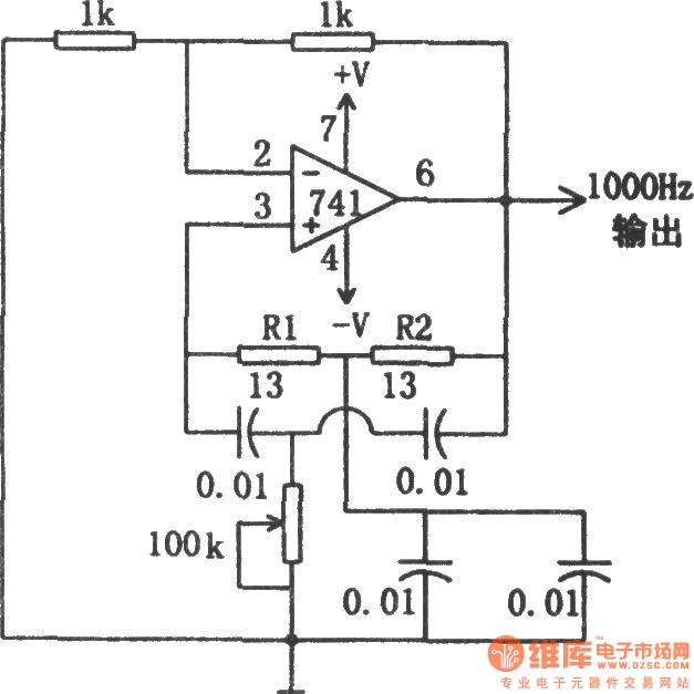
1kHz sine wave oscillator(741)
The circuit illustrated in the diagram is a 1 kHz sine wave oscillator circuit. Based on a double-T circuit configuration, it utilizes a standard 741 operational amplifier to generate a 1000 Hz sine wave output. The circuit begins oscillation when...
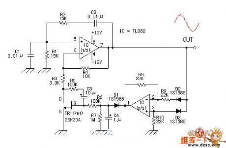
Sine Signal Generating
The circuit is capable of changing the frequency range, with the oscillating signal adjustable via potentiometer RP1. The output resistance is low (1 kΩ), making it suitable for various control circuit applications as a signal source. In this design, the...
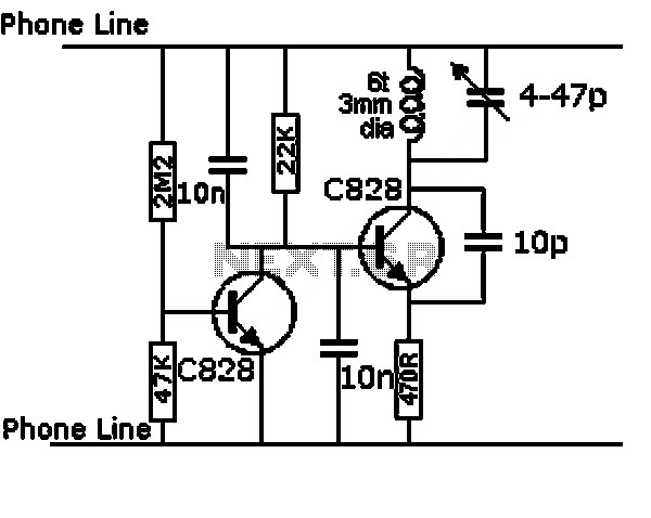
tuned sine wave oscillator circuit
This design circuit is intended for sine wave oscillators, providing both sine and square wave outputs across a frequency range from below 20 Hz to above 20 KHz. The oscillation frequency can be easily adjusted by changing a single resistor....
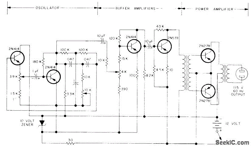
100W SINE AT 60Hz
The circuit primarily comprises a 60-Hz sine-wave oscillator featuring a 10K frequency-control potentiometer, two buffering stages, and a push-pull power amplifier. This design effectively addresses the noise issues associated with square-wave inverters, particularly when powering a 115-V radio receiver or...
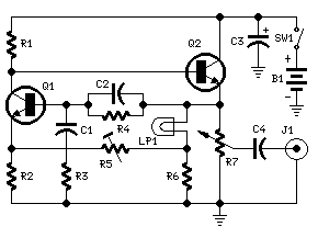
1KHz Sine wave Generator
This circuit generates a good 1KHz sinewave adopting the inverted Wien bridge configuration (C1-R3 & C2-R4). It features a variable output, low distortion and low output impedance in order to obtain good overload capability. A small filament bulb ensures a...
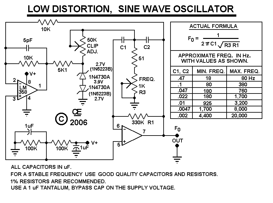
A Simple Sine Wave Oscillator
After constructing the device, adjust the frequency to the desired level using the "Frequency Control." Then, utilize an oscilloscope to fine-tune the waveform for optimal performance with the "Clip Control." The sharp rise and fall times of square waves cause...
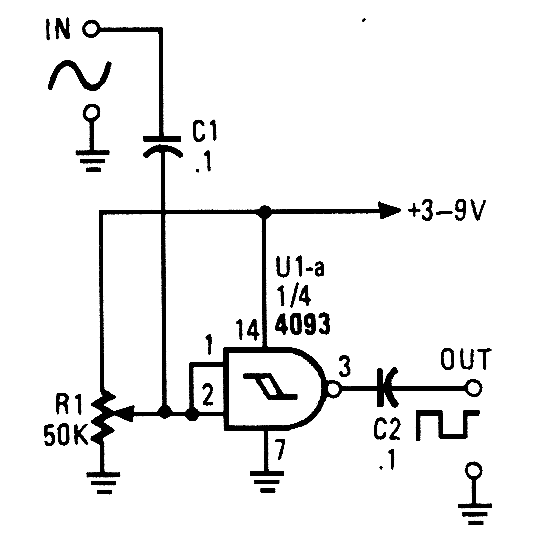
SINE WAVE TO SQUARE WAVE CONVERTER
This circuit converts a sine wave into a square wave. It consists of a single 2-input NAND Schmitt trigger configured as an inverter, with a trigger level adjustment at its input. As the input voltage exceeds the gate's trigger point,...
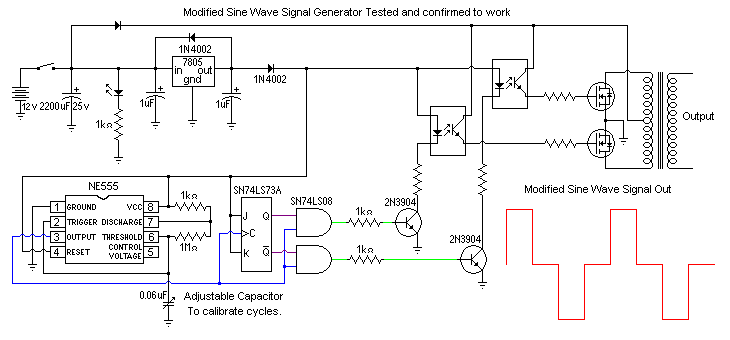
Modified Sine Wave Signal Generator
Pure sine wave inverters are optimal; however, they are costly to purchase or construct. Modified sine wave inverters can power certain equipment, while square wave inverters have more limitations.
Pure sine wave inverters are highly regarded for their ability to produce...
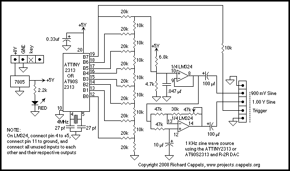
Digital Sine Wave Oscillator
If found myself in need of a 1 KHz signal source for an experiments. My function/sweep generator was needed as a pulse generator for the same experiment, so I went though my junk box, looking for circuits from long ago...