


shootout volume 5 paralleling egan fets part 2
#eGaN FETs
#buck converter
#half bridge
#power electronics
#high frequency
#parallel devices
#voltage conversion
#switching circuits
#EPC2001
#1MHz
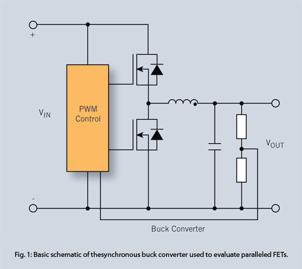
Description: The first part of this two-part article on paralleling eGaN FETs introduced five basic designs that utilized four EPC2001 (100 V, 25 A) paralleled devices per switch in a half-bridge configuration, accompanied by experimental validation. The second part demonstrates a 1 MHz buck converter employing two parallel eGaN FETs, showcasing exceptional performance compared to state-of-the-art silicon devices in a similar circuit.
The design of a buck converter using eGaN FETs highlights the advantages of using gallium nitride (GaN) technology over traditional silicon solutions, particularly in high-frequency applications. The buck converter operates at a switching frequency of 1 MHz, which allows for smaller passive components and improved power density. The use of two parallel EPC2001 devices ensures that the current handling capability is maximized while minimizing the on-resistance and switching losses that typically plague silicon-based designs.
In this configuration, the half-bridge topology is employed, which consists of two switches (the eGaN FETs) and a diode. The parallel arrangement of the FETs not only enhances the overall current capacity but also balances the thermal and electrical characteristics across the devices, leading to improved efficiency and reliability.
The experimental validation of the circuit design demonstrates its effectiveness in achieving high efficiency, low electromagnetic interference (EMI), and excellent thermal performance. The results indicate that the eGaN FETs outperform their silicon counterparts in terms of efficiency at 1 MHz, with lower conduction and switching losses contributing to overall system performance.
Furthermore, the layout of the PCB is critical in high-frequency applications, requiring careful attention to minimize parasitic inductances and capacitances. The design should incorporate short traces, proper grounding techniques, and adequate heat dissipation measures to ensure optimal performance of the eGaN FETs.
In conclusion, the use of parallel eGaN FETs in a 1 MHz buck converter showcases the potential for GaN technology to redefine performance benchmarks in power electronics, particularly in applications demanding high efficiency and compact size. The findings from this study pave the way for further exploration into the capabilities of eGaN devices in advanced power conversion systems.In the first installment of this two-part article on paralleling eGaN FETs, five basic designs, utilizing four EPC2001 (100 V, 25 A) paralleled devices per switch in a half bridge configuration were presented with experimental validation. In this second installment, a 1MHz buck converter is demonstrated using two parallel eGaN FETs with exceptional performance compared, with state-of-the-art silicon devices in a similar circuit..
The design of a buck converter using eGaN FETs highlights the advantages of using gallium nitride (GaN) technology over traditional silicon solutions, particularly in high-frequency applications. The buck converter operates at a switching frequency of 1 MHz, which allows for smaller passive components and improved power density. The use of two parallel EPC2001 devices ensures that the current handling capability is maximized while minimizing the on-resistance and switching losses that typically plague silicon-based designs.
In this configuration, the half-bridge topology is employed, which consists of two switches (the eGaN FETs) and a diode. The parallel arrangement of the FETs not only enhances the overall current capacity but also balances the thermal and electrical characteristics across the devices, leading to improved efficiency and reliability.
The experimental validation of the circuit design demonstrates its effectiveness in achieving high efficiency, low electromagnetic interference (EMI), and excellent thermal performance. The results indicate that the eGaN FETs outperform their silicon counterparts in terms of efficiency at 1 MHz, with lower conduction and switching losses contributing to overall system performance.
Furthermore, the layout of the PCB is critical in high-frequency applications, requiring careful attention to minimize parasitic inductances and capacitances. The design should incorporate short traces, proper grounding techniques, and adequate heat dissipation measures to ensure optimal performance of the eGaN FETs.
In conclusion, the use of parallel eGaN FETs in a 1 MHz buck converter showcases the potential for GaN technology to redefine performance benchmarks in power electronics, particularly in applications demanding high efficiency and compact size. The findings from this study pave the way for further exploration into the capabilities of eGaN devices in advanced power conversion systems.In the first installment of this two-part article on paralleling eGaN FETs, five basic designs, utilizing four EPC2001 (100 V, 25 A) paralleled devices per switch in a half bridge configuration were presented with experimental validation. In this second installment, a 1MHz buck converter is demonstrated using two parallel eGaN FETs with exceptional performance compared, with state-of-the-art silicon devices in a similar circuit..
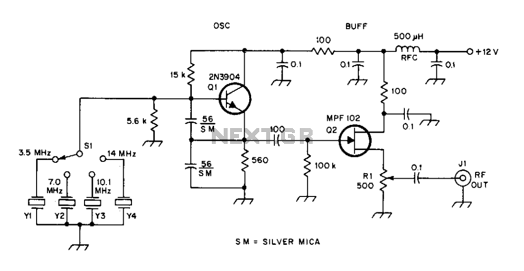
High frequency signal generator
A tapped-coil Colpitts oscillator is utilized at Q1 to deliver four tuning ranges: 1.7 to 3.131 MHz, 3.0 to 5.6 MHz, 5.0 to 12 MHz, and 11.5 to 31 MHz. A Zener diode (D2) is incorporated at Q1 to reduce...
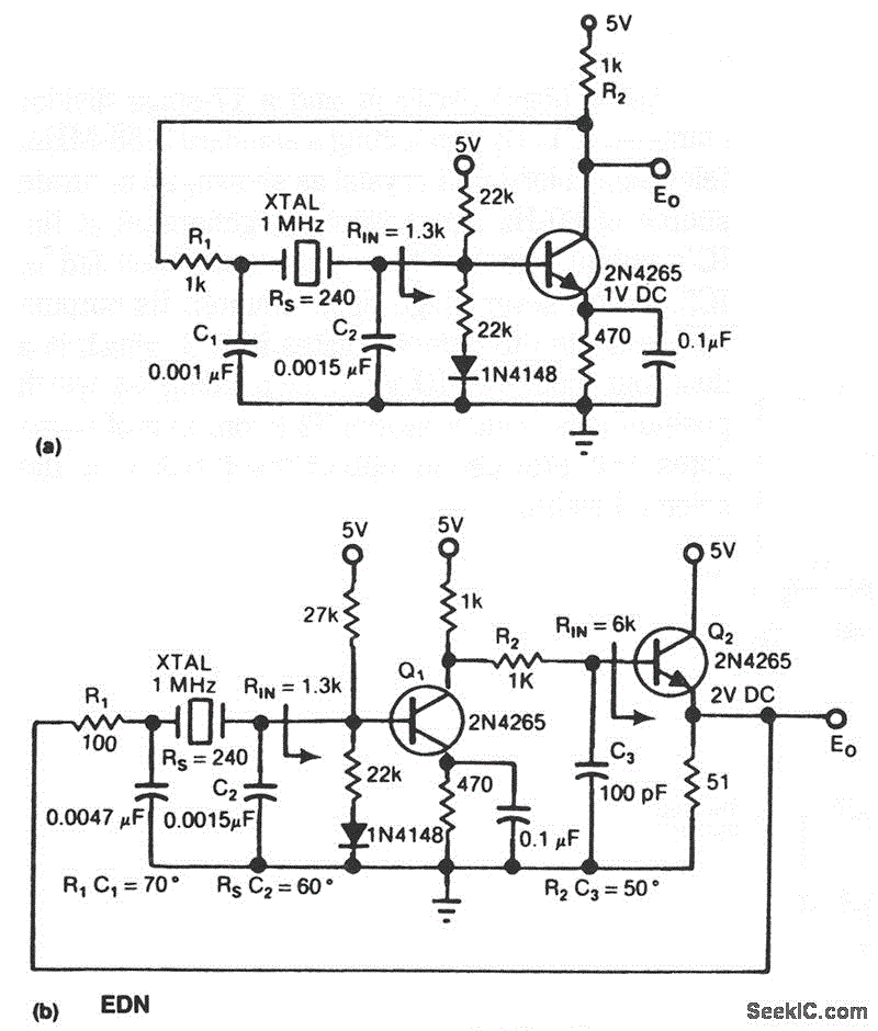
1MHz PIERCE OSCILLATORS
A simple network design is a key feature of the Pierce circuit, as illustrated by these 1-MHz oscillators. Operating the crystal slightly above resonance requires only one high-gain transistor stage. Operating it exactly at series resonance requires an additional RC...
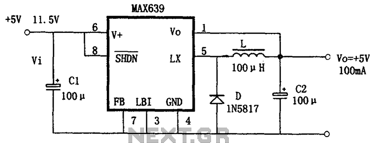
Buck power conversion by the MAX639 + 5V fixed output
The circuit is based on the MAX639, which is a high-efficiency, step-down DC/DC converter. It operates with an input voltage range of 5.5V to 11.5V, providing a fixed output voltage of +5V or an adjustable voltage. The output current capability...
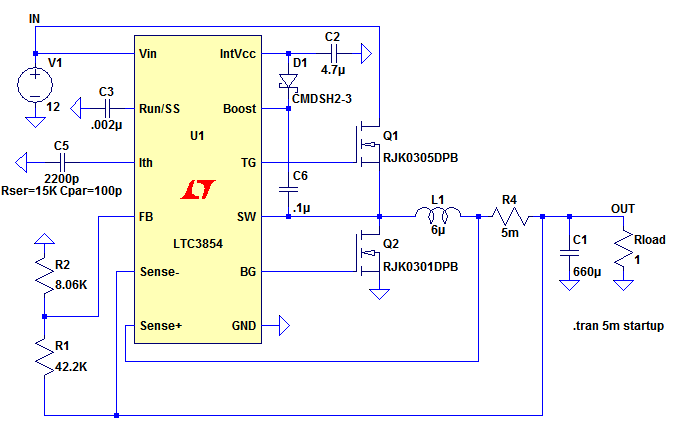
Buck Converter Design
The top MOSFET activates, creating a short circuit between the input voltage (IN) and the left side of the inductor, L1. The inductor current increases according to the equation where V is the voltage across the inductor, L is the...
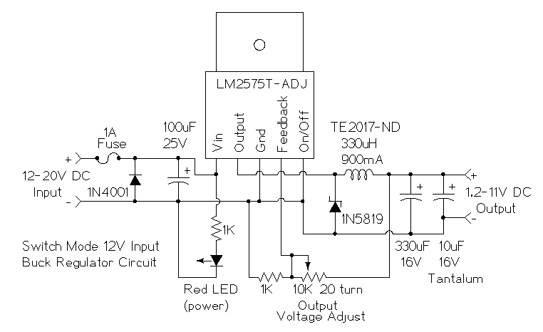
Simple buck mode switching regulator circuit diagram
This is a simple buck mode switching regulator circuit diagram. This circuit is more efficient; switch mode regulators convert DC input voltage to pulses of high DC voltage. The DC pulses are used to charge a storage capacitor to the...
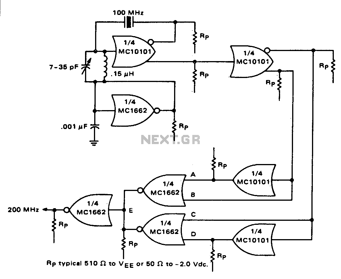
High frequency crystal oscillator
One section of the MC10101 is configured as a 100 MHz crystal oscillator, with the crystal placed in series within the feedback loop. An LC tank circuit is utilized to tune the 100 MHz harmonic of the crystal, which can...
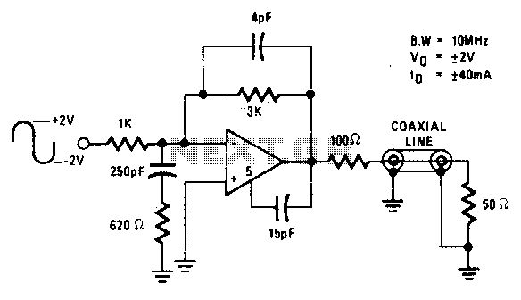
10Mhz coaxial line driver
The circuit is ideal for high-frequency line driving systems that necessitate a wide power bandwidth at elevated output current levels. The integrated circuit used is HA2530. The bandwidth of the circuit is constrained solely by the single pole response of...
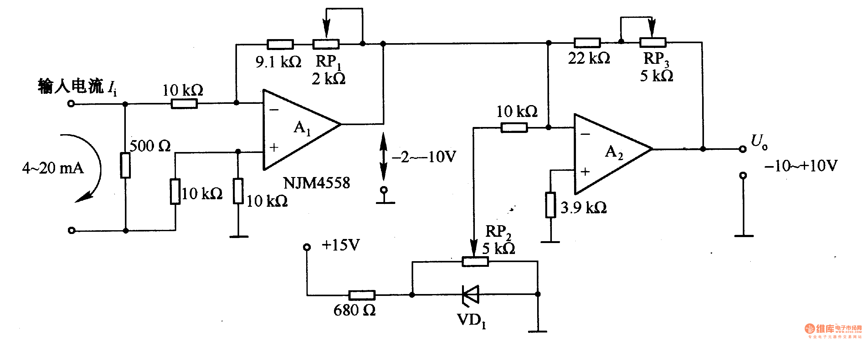
voltage conversion circuit composed of NJM4558
Figure 1-42 (a) is a voltage/current conversion circuit that converts a 0-10V input voltage into a 4-20mA output current. Adjusting resistor RP2 can set the input voltage (Ui) to 0V, resulting in an output current (I) of 20mA; similarly, setting...
Buck Converter Design
The top MOSFET activates, creating a short circuit between the input voltage (IN) and the left side of the inductor, L1. The inductor current increases according to the equation where V is the voltage across the inductor, L is the...