


Machine vision illumination stabilizer
#hysteresis oscillator
#lamp illumination
#CMOS Schmitt trigger
#voltage stabilization
#transistor control
#AC line operation
#unregulated DC
#zener diode
#logic threshold
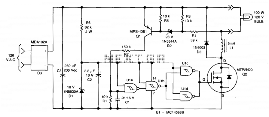
Description: The combination of Q1, Q2, and U1 forms a hysteresis oscillator that stabilizes lamp illumination. In operation, a full-wave bridge rectifier D3 operates directly from the AC line to supply unregulated DC to the lamp and to the 10 V zener diode that powers the quad CMOS Schmitt trigger, U1. When the lamp supply exceeds 115 V, Q1 is turned ON, charging C1 through R2 to raise the input to U1A past the positive-going logic threshold. This causes the output voltage at U1C and U1D to drop, which drives the gate of Q2, turning it OFF.
Current then decays through the lamp, L1, and D3 until the lamp voltage falls below 115 V, at which point Q1 turns OFF and the cycle repeats.
The circuit employs a hysteresis oscillator configuration, utilizing transistor Q1, Q2, and operational amplifier U1 to maintain stable illumination of a lamp. The full-wave bridge rectifier D3 converts the incoming AC voltage to unregulated DC voltage, which is essential for powering both the lamp and the associated control circuitry. The 10 V zener diode serves as a voltage reference, ensuring that the CMOS Schmitt trigger operates within its specified range, providing reliable switching behavior.
When the voltage across the lamp exceeds 115 V, Q1 is activated, allowing current to flow through charging capacitor C1 via resistor R2. This charging process increases the voltage at the input of U1A until it surpasses the threshold voltage, triggering a response from the Schmitt trigger. The output from U1C and U1D subsequently goes low, which in turn signals Q2 to turn OFF, interrupting the current flow through the lamp.
As the current through the lamp decreases, the voltage across the lamp drops. This continues until the voltage falls below the critical threshold of 115 V, at which point Q1 deactivates, and the entire process starts anew. This feedback mechanism ensures that the lamp remains illuminated at a stable brightness, preventing flickering and enhancing the longevity of the lamp by avoiding excessive voltage conditions.
The design emphasizes efficiency by utilizing components that are well-suited for the intended application, such as the CMOS technology in the Schmitt trigger for low power consumption and rapid switching capabilities. The hysteresis effect provides noise immunity, ensuring stable operation even in the presence of voltage fluctuations. Overall, this circuit exemplifies a robust solution for maintaining consistent lamp illumination in various lighting applications.The combination of Ql, Q2 and Ul form a hysteresis oscillator to stabilize lamp illumination. In operation, full wave bridge D3 operates directly from the ac line to supply unregulated dc to the lamp and also to the 10 V zener that provides power to the quad CMOS Schmitt trigger, Ul. When the lamp supply exceeds 115 V, Ql is turned ON, charging Cl through R2 to raise the input to Ula past the positive-going logic threshold.
This drops the output voltage at Ulc and Uld, which drives the gate of Q2, turning it OFF. Current then decays through the lamp, LI and D3 until the lamp voltage falls below 115 V, at which time Ql turns OFF and the cycle repeats.
Current then decays through the lamp, L1, and D3 until the lamp voltage falls below 115 V, at which point Q1 turns OFF and the cycle repeats.
The circuit employs a hysteresis oscillator configuration, utilizing transistor Q1, Q2, and operational amplifier U1 to maintain stable illumination of a lamp. The full-wave bridge rectifier D3 converts the incoming AC voltage to unregulated DC voltage, which is essential for powering both the lamp and the associated control circuitry. The 10 V zener diode serves as a voltage reference, ensuring that the CMOS Schmitt trigger operates within its specified range, providing reliable switching behavior.
When the voltage across the lamp exceeds 115 V, Q1 is activated, allowing current to flow through charging capacitor C1 via resistor R2. This charging process increases the voltage at the input of U1A until it surpasses the threshold voltage, triggering a response from the Schmitt trigger. The output from U1C and U1D subsequently goes low, which in turn signals Q2 to turn OFF, interrupting the current flow through the lamp.
As the current through the lamp decreases, the voltage across the lamp drops. This continues until the voltage falls below the critical threshold of 115 V, at which point Q1 deactivates, and the entire process starts anew. This feedback mechanism ensures that the lamp remains illuminated at a stable brightness, preventing flickering and enhancing the longevity of the lamp by avoiding excessive voltage conditions.
The design emphasizes efficiency by utilizing components that are well-suited for the intended application, such as the CMOS technology in the Schmitt trigger for low power consumption and rapid switching capabilities. The hysteresis effect provides noise immunity, ensuring stable operation even in the presence of voltage fluctuations. Overall, this circuit exemplifies a robust solution for maintaining consistent lamp illumination in various lighting applications.The combination of Ql, Q2 and Ul form a hysteresis oscillator to stabilize lamp illumination. In operation, full wave bridge D3 operates directly from the ac line to supply unregulated dc to the lamp and also to the 10 V zener that provides power to the quad CMOS Schmitt trigger, Ul. When the lamp supply exceeds 115 V, Ql is turned ON, charging Cl through R2 to raise the input to Ula past the positive-going logic threshold.
This drops the output voltage at Ulc and Uld, which drives the gate of Q2, turning it OFF. Current then decays through the lamp, LI and D3 until the lamp voltage falls below 115 V, at which time Ql turns OFF and the cycle repeats.

Zener Tester schematic
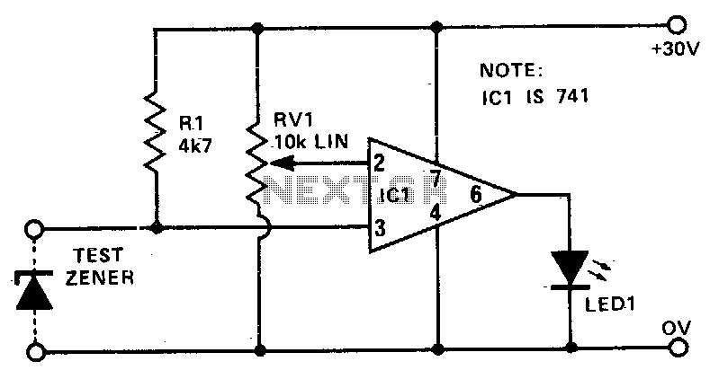
With this simple measuring device can: Determine the Zener voltage up to 25V. The connections of cathode and anode of each diode finding. Check if a diode fails. Silicon, germanium and Schottky diodes distinguish. LED test and the V forward...
Zener tester
This circuit offers a cost-effective and dependable method for testing zener diodes. The variable resistor RV1 can be calibrated in volts, allowing the user to determine the zener voltage directly by observing when LED 1 begins to illuminate. At this...
Simple Zener Diode Tester
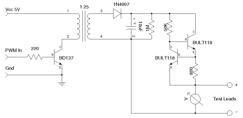
A simple Zener diode tester circuit, when combined with a PWM generator, can be utilized to measure the breakdown voltage of Zener diodes. More generally, it can also measure the breakdown voltages (e.g., BVceo, BVcbo) of BJTs (Bipolar Junction Transistors)....
I/O Line Protectors
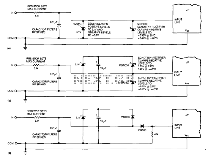
A 5.1-V zener diode is utilized to clamp positive-going transients, while a Schottky rectifier is employed to clamp negative-going transients. The Schottky rectifier, however, experiences issues at both extremes of the temperature range. At 125°C (257°F), its leakage current can...
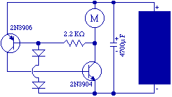
Zener-based solar engine
The capacitor charges until the PNP transistor (here shown as a 2N3906, but you could also use a BC327) receives base current through the Zener and turns on. Then the NPN transistor (here shown as a 2N3904, but you could...
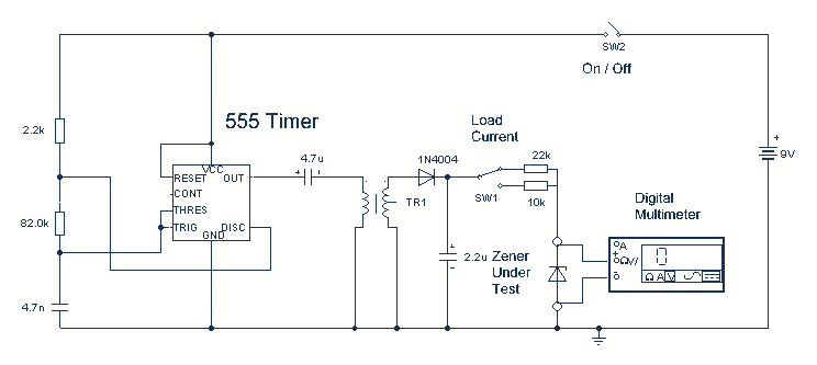
Zener Diode Tester
Using a single 555 Timer IC and a small transformer to generate a high voltage, this circuit will test zener diodes of voltage ratings up to 50VDC. The 555 timer is used in the astable mode, the output at pin3...
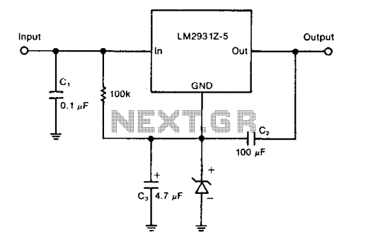
Zener diode increase regulator output
A zener diode in the ground lead of a fixed PNP regulator varies the voltage output of that device without a significant sacrifice in regulation. The technique also allows the regulator to operate with output voltages beyond its rated limit.
The...
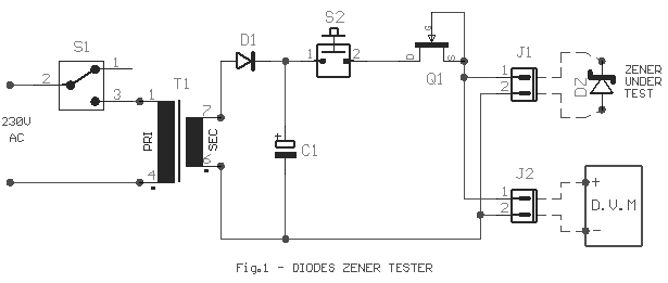
diode zener tester
Frequently, there are situations where the need arises to utilize a Zener diode, yet the operational voltage is unknown. Often, the characteristics or type inscribed on the diode are not legible.
Zener diodes are essential components in electronic circuits, primarily used...
Zener-based solar engine
The capacitor charges until the PNP transistor (here shown as a 2N3906, but you could also use a BC327) receives base current through the Zener and turns on. Then the NPN transistor (here shown as a 2N3904, but you could...