


Synchronous Camera Flash Trigger Using IGBT
#camera flash
#IGBT
#trigger circuit
#photography
#synchronization
#SCR
#pulse width
#electronic flash
#photo equipment
#light control
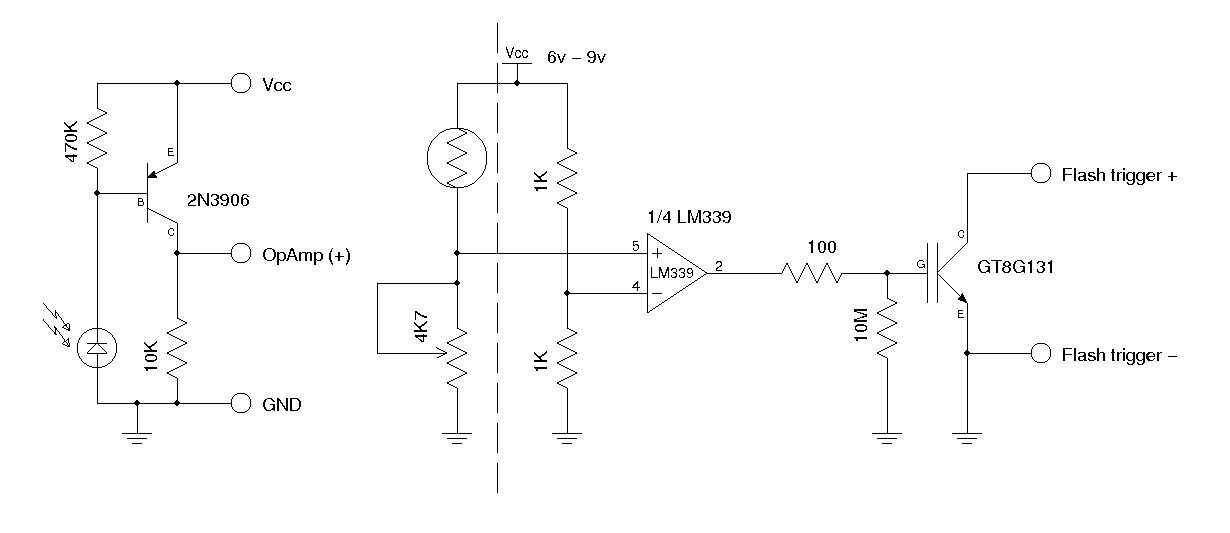
Description: A synchronous camera flash, such as a slave flash, is typically triggered using a silicon-controlled rectifier (SCR). This document presents a circuit designed to trigger a secondary camera flash utilizing an insulated-gate bipolar transistor (IGBT). The use of an IGBT for triggering a camera flash offers several advantages over the conventional SCR method, including precise control over the width of the triggering pulse, which enables functionalities such as red-eye prevention that are not easily achievable with SCR-triggered circuits. Depending on the camera model, the light sensor can be a cadmium sulfide (CdS) photoresistor, a photodiode, or a phototransistor. For many automatic cameras, a photodiode or phototransistor may be necessary due to the faster shutter speeds that exceed the response time of a CdS sensor. The circuit schematic illustrates the compatibility of both types of sensors. The operation of this circuit is as follows: the inverting input of the comparator (LM339) is set to approximately Vcc/2. When the CdS sensor detects the primary camera flash, its resistance decreases, causing the voltage at the non-inverting input to surpass the reference voltage. The comparator then outputs a high signal (close to Vcc), which triggers the IGBT. The IGBT in this design is a Toshiba GT8G131 N-channel IGBT, specifically tailored for strobe flash applications. It is crucial to provide a sufficiently high gate voltage, within safe limits, to ensure the IGBT is fully activated. Insufficient gate voltage may prevent the IGBT from conducting enough current to trigger the flash tube. Therefore, adjustments to Vcc may be necessary when using different IGBT types.
The circuit operates by utilizing a comparator to detect the primary flash and subsequently trigger the secondary flash via the IGBT. The LM339 comparator is chosen for its low input offset voltage, which enhances the accuracy of the triggering process. The circuit design includes a resistor divider network that sets the reference voltage at the inverting input, ensuring that it remains stable during operation.
When the primary flash occurs, the light sensor (CdS, photodiode, or phototransistor) detects the light intensity, leading to a rapid decrease in resistance. This change in resistance results in an increase in voltage at the non-inverting input of the comparator. Once this voltage exceeds the reference voltage, the comparator output switches to a high state, activating the gate of the IGBT.
The Toshiba GT8G131 IGBT is selected for its high-speed switching capabilities and robustness under high current conditions, making it ideal for flash applications. It is essential to ensure that the gate voltage applied to the IGBT is adequate to fully turn it on; typically, this voltage should be around 10-15 volts for optimal performance. If the voltage is too low, the IGBT may not enter the saturation region, resulting in insufficient current flow to trigger the flash tube effectively.
In summary, this circuit provides a reliable and efficient method for triggering a secondary camera flash, utilizing the advantages of IGBT technology while ensuring compatibility with various light sensors and camera models. Proper attention to the gate voltage and component selection is crucial for the successful operation of this flash triggering circuit.Typically a synchronous camera flash (e. g. slave flash) is triggered via an SCR. In this blog post, I will show you a circuit that can be used to trigger a secondary camera flash using an IGBT. Using an IGBT for camera flash triggering has several advantages over the traditional SCR triggering mechanism: for instance, the width of the triggering pulse can
be controlled precisely and thus enabling functions such as red eye prevention that cannot be achieved easily using an SCR triggered circuit. Depending on the camera used, the light sensor can be either a CdS photoresistor, a photodiode or a phototransistor.
For many automatic cameras, a photodiode or photo transistor maybe necessary as the shutter speed is typically faster than then reaction time of a CdS sensor. The schematics above also shows how both types of sensors can be used. Here is how this circuit works. The inverting input of the comparator (LM339) is referenced at roughly Vcc/2. When the CdS sensor detects the primary camera flash, its resistance drops and the voltage at the none-inverting input exceeds the reference voltage.
The comparator output a high (e. g. close to Vcc) and thus triggers the IGBT. The IGBT used here is a Toshiba GT8G131 N Channel IGBT, which is specifically designed for strobe flash applications. It is important to supply a high enough (within safety limit) gate voltage to ensure that the IGBT is fully turned on.
Otherwise, the IGBT may not be able to conduct a high enough current to trigger the flash tube. So if you are using other types of IGBT, you may need to adjust the Vcc accordingly.
The circuit operates by utilizing a comparator to detect the primary flash and subsequently trigger the secondary flash via the IGBT. The LM339 comparator is chosen for its low input offset voltage, which enhances the accuracy of the triggering process. The circuit design includes a resistor divider network that sets the reference voltage at the inverting input, ensuring that it remains stable during operation.
When the primary flash occurs, the light sensor (CdS, photodiode, or phototransistor) detects the light intensity, leading to a rapid decrease in resistance. This change in resistance results in an increase in voltage at the non-inverting input of the comparator. Once this voltage exceeds the reference voltage, the comparator output switches to a high state, activating the gate of the IGBT.
The Toshiba GT8G131 IGBT is selected for its high-speed switching capabilities and robustness under high current conditions, making it ideal for flash applications. It is essential to ensure that the gate voltage applied to the IGBT is adequate to fully turn it on; typically, this voltage should be around 10-15 volts for optimal performance. If the voltage is too low, the IGBT may not enter the saturation region, resulting in insufficient current flow to trigger the flash tube effectively.
In summary, this circuit provides a reliable and efficient method for triggering a secondary camera flash, utilizing the advantages of IGBT technology while ensuring compatibility with various light sensors and camera models. Proper attention to the gate voltage and component selection is crucial for the successful operation of this flash triggering circuit.Typically a synchronous camera flash (e. g. slave flash) is triggered via an SCR. In this blog post, I will show you a circuit that can be used to trigger a secondary camera flash using an IGBT. Using an IGBT for camera flash triggering has several advantages over the traditional SCR triggering mechanism: for instance, the width of the triggering pulse can
be controlled precisely and thus enabling functions such as red eye prevention that cannot be achieved easily using an SCR triggered circuit. Depending on the camera used, the light sensor can be either a CdS photoresistor, a photodiode or a phototransistor.
For many automatic cameras, a photodiode or photo transistor maybe necessary as the shutter speed is typically faster than then reaction time of a CdS sensor. The schematics above also shows how both types of sensors can be used. Here is how this circuit works. The inverting input of the comparator (LM339) is referenced at roughly Vcc/2. When the CdS sensor detects the primary camera flash, its resistance drops and the voltage at the none-inverting input exceeds the reference voltage.
The comparator output a high (e. g. close to Vcc) and thus triggers the IGBT. The IGBT used here is a Toshiba GT8G131 N Channel IGBT, which is specifically designed for strobe flash applications. It is important to supply a high enough (within safety limit) gate voltage to ensure that the IGBT is fully turned on.
Otherwise, the IGBT may not be able to conduct a high enough current to trigger the flash tube. So if you are using other types of IGBT, you may need to adjust the Vcc accordingly.
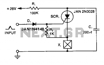
Squib-firing circuit
Capacitor C1 is charged to +28 V through resistor R1 and stores energy for firing the squib. A positive pulse of 1 mA applied to the gate of SCR1 will cause it to conduct, discharging C1 into the squib load...
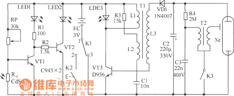
Camera internal flash circuit
This circuit consists of a light measurement circuit and a flash circuit, as illustrated in the accompanying figure. It is applicable in the POPTICS (a popular integrated camera), the Franka X-500, and the WIZEN-860S cameras. The light measurement circuit includes...
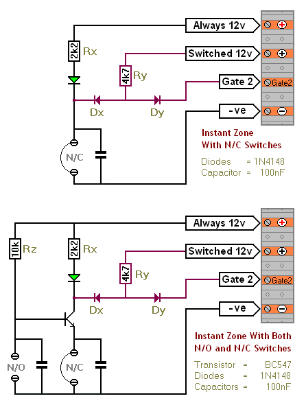
An SCR Based Burglar Alarm - Adding Extra Zones
The SCR Burglar Alarm System allows for the addition of multiple extra zones. The primary circuit is designed for typical normally-closed input devices, including magnetic reed contacts, micro switches, foil tape, and passive infrared (PIR) sensors. An additional circuit includes...
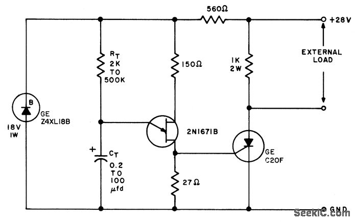
SCR UJI TIME DELAY
The timing interval is initiated by applying power and is determined by the resistor-capacitor (RT-CT) combination. At the end of the interval, a unijunction transistor triggers a silicon controlled rectifier (SCR) to apply nearly the full supply voltage to the...
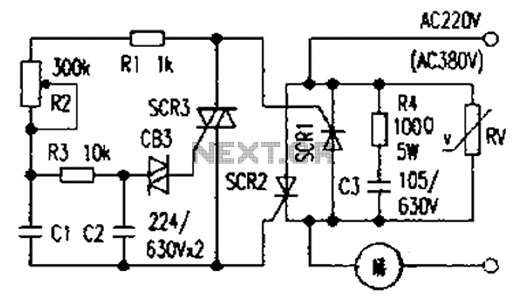
Simple and practical power SCR trigger circuit diagram
The presentation of a general power thyristor trigger circuit is more complex, and some components are difficult to procure. A successful trigger circuit has been constructed for only a few dollars. This circuit is designed to trigger a thyristor module...
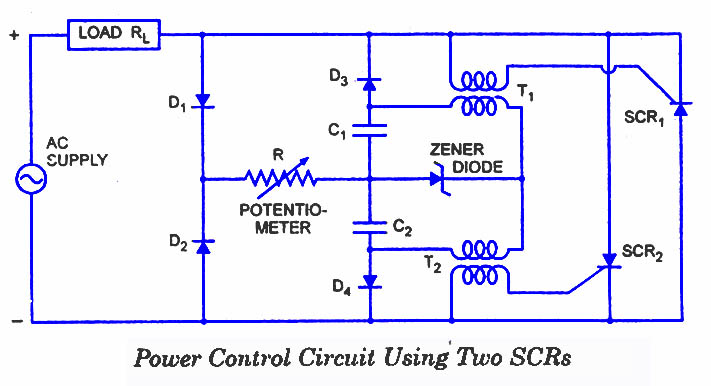
SCR Applications
The ability of an SCR to control large currents to a load using a small gate current makes the device highly useful in switching and control applications. Several potential applications for the SCR include power control, switching, zero-voltage switching, over-voltage...
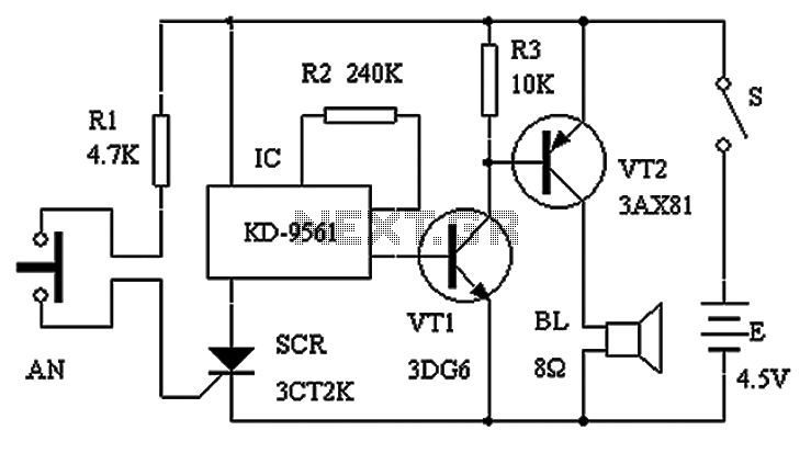
Normally closed contact burglar alarm circuit diagram
The circuit schematic presented in Figure 1 consists of an SCR, R1, and an AN SCR trigger switch circuit, along with an analog circuit composed of IC1, R2, VT1, VT2, and a BL siren. Typically, the circuit is designed to...
Scr Capacitor Turn-Off Circuit
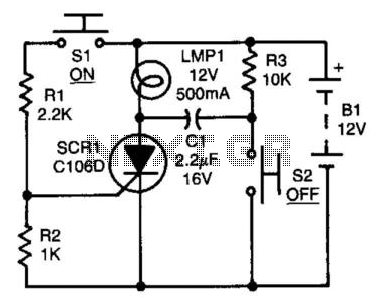
After the SCR is activated, capacitor CI charges up to nearly the full supply voltage through resistor R3 and the anode of the SCR. When switch S2 is later closed, it grounds the positive terminal of CI, causing the charge...
scr tester
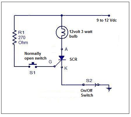
Although SCRs and TRIACs are not present in all electronic equipment, they are significant components. Understanding how to test them is essential for troubleshooting. Testing these components can be done with meters, but using an SCR/TRIAC tester is generally easier...