


14 Bit A-D Converter with ICL7134B
#A-D converter
#ICL7134B
#successive approximation
#14-bit
#comparator
#HA2605
#auto-zero circuit
#ICL7650
#TTL Schmitt trigger
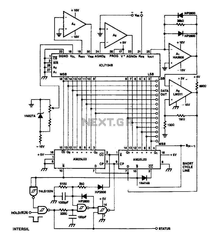
Description: The ICL7134B circuit is a bipolar input analog-to-digital (A/D) converter that employs two AM25L03 chips to create a 14-bit successive approximation register. The comparator features a two-stage amplifier, HA2605, which is utilized to mitigate settling time issues at the summing node. It is important to address the nulling offset of this amplifier, and for applications requiring a wide temperature range, an auto-zero circuit using the ICL7650 is recommended. The clock circuit, composed of two TTL Schmitt trigger gates, operates at a slower rate during the first 8 bits, where settling time is more critical compared to the final 6 bits.
The circuit operates in a free-running mode when the HOLD/RUN input is low; however, it halts after completing a conversion if the pin is high at that moment. A low pulse can be used to restart the operation. The exit status provides information on whether the device is active, with the falling edge indicating the availability of new data. A unipolar version can be constructed by connecting the most significant bit (D13) of the ICL7134U to pin 14 of the first AM25L03, removing the reference inversion amplifier A4, and connecting to VRFM and VRFL.
The circuit design involves several key components and configurations that ensure accurate data conversion and reliable performance. The ICL7134B serves as the core A/D converter, utilizing its internal architecture to achieve high resolution and precision. The AM25L03 chips function as successive approximation registers, allowing for efficient conversion of analog signals to digital representations.
The HA2605 amplifier plays a critical role in enhancing the performance of the comparator by reducing settling time, which is essential for maintaining the integrity of the conversion process. The incorporation of an auto-zero circuit using the ICL7650 is particularly advantageous in applications subjected to varying temperature conditions, as it helps maintain accuracy by compensating for offset errors.
The clock circuit's design, utilizing TTL Schmitt triggers, is optimized for the differing settling time requirements of the initial and subsequent bits. This careful timing strategy ensures that the most critical bits are processed with the utmost precision, thereby improving overall conversion accuracy.
The HOLD/RUN input functionality provides flexibility in the circuit's operation, allowing it to either continuously convert data or pause and restart based on external control signals. This feature is particularly useful in applications where data acquisition needs to be synchronized with other system components.
The option to configure the circuit for unipolar operation expands its applicability, making it suitable for a wider range of signal types. By modifying the connections and removing specific components, the circuit can be adapted to meet the specific requirements of various measurement and control tasks.
Overall, the ICL7134B-based circuit represents a sophisticated solution for high-resolution analog-to-digital conversion, combining advanced components and thoughtful design to achieve reliable performance across diverse applications.The circuit ICL7134B base is a bipolar input AID converter broadband, using two AM25L03s to form a successive approximation register 14-bit. The comparator is a circuit with two stage amplifier HA2605 front, used to reduce the settling time problems in the pro summing node (see A020).
Warning nu11ing offset of this amplifier is needed and if wide temperature range operation is desired, an auto-zero circuit using a lCL7650 is probably desirable (see A053). The clock, using two gates TTL Schmitt trigger operates at a slower pace for the first 8 bits, where the settlement time is more critical than for the last 6 bits.
The line is short-cycle showed little tied at 15, if fewer bits are needed, it can be moved accordingly. The circuit will free run if the HOLD / RUN input low, but stops after performing a conversion if the pin is high at this time.
a low pulse will restart it. The exit status indicates whether the device is operating, and the falling edge indicates the availability of new data. Unipolar version can be built by typing the MSB (D13) on a ICL7134U to pin 14 on the first AM25L03, deleting the reference inversion amplifier A4, and attaching to VRFM VRFL.
The line is short-cycle showed little tied at 15, if fewer bits are needed, it can be moved accordingly. The circuit will free run if the HOLD / RUN input low, but stops after performing a conversion if the pin is high at this time.
a low pulse will restart it. The exit status indicates whether the device is operating, and the falling edge indicates the availability of new data.
The circuit operates in a free-running mode when the HOLD/RUN input is low; however, it halts after completing a conversion if the pin is high at that moment. A low pulse can be used to restart the operation. The exit status provides information on whether the device is active, with the falling edge indicating the availability of new data. A unipolar version can be constructed by connecting the most significant bit (D13) of the ICL7134U to pin 14 of the first AM25L03, removing the reference inversion amplifier A4, and connecting to VRFM and VRFL.
The circuit design involves several key components and configurations that ensure accurate data conversion and reliable performance. The ICL7134B serves as the core A/D converter, utilizing its internal architecture to achieve high resolution and precision. The AM25L03 chips function as successive approximation registers, allowing for efficient conversion of analog signals to digital representations.
The HA2605 amplifier plays a critical role in enhancing the performance of the comparator by reducing settling time, which is essential for maintaining the integrity of the conversion process. The incorporation of an auto-zero circuit using the ICL7650 is particularly advantageous in applications subjected to varying temperature conditions, as it helps maintain accuracy by compensating for offset errors.
The clock circuit's design, utilizing TTL Schmitt triggers, is optimized for the differing settling time requirements of the initial and subsequent bits. This careful timing strategy ensures that the most critical bits are processed with the utmost precision, thereby improving overall conversion accuracy.
The HOLD/RUN input functionality provides flexibility in the circuit's operation, allowing it to either continuously convert data or pause and restart based on external control signals. This feature is particularly useful in applications where data acquisition needs to be synchronized with other system components.
The option to configure the circuit for unipolar operation expands its applicability, making it suitable for a wider range of signal types. By modifying the connections and removing specific components, the circuit can be adapted to meet the specific requirements of various measurement and control tasks.
Overall, the ICL7134B-based circuit represents a sophisticated solution for high-resolution analog-to-digital conversion, combining advanced components and thoughtful design to achieve reliable performance across diverse applications.The circuit ICL7134B base is a bipolar input AID converter broadband, using two AM25L03s to form a successive approximation register 14-bit. The comparator is a circuit with two stage amplifier HA2605 front, used to reduce the settling time problems in the pro summing node (see A020).
Warning nu11ing offset of this amplifier is needed and if wide temperature range operation is desired, an auto-zero circuit using a lCL7650 is probably desirable (see A053). The clock, using two gates TTL Schmitt trigger operates at a slower pace for the first 8 bits, where the settlement time is more critical than for the last 6 bits.
The line is short-cycle showed little tied at 15, if fewer bits are needed, it can be moved accordingly. The circuit will free run if the HOLD / RUN input low, but stops after performing a conversion if the pin is high at this time.
a low pulse will restart it. The exit status indicates whether the device is operating, and the falling edge indicates the availability of new data. Unipolar version can be built by typing the MSB (D13) on a ICL7134U to pin 14 on the first AM25L03, deleting the reference inversion amplifier A4, and attaching to VRFM VRFL.
The line is short-cycle showed little tied at 15, if fewer bits are needed, it can be moved accordingly. The circuit will free run if the HOLD / RUN input low, but stops after performing a conversion if the pin is high at this time.
a low pulse will restart it. The exit status indicates whether the device is operating, and the falling edge indicates the availability of new data.
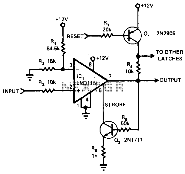
Comparator-latch
The main advantage of this circuit, in comparison to other comparators, is its capability to latch once the input surpasses a specified threshold level. When the input goes beyond this threshold, the output of the LM311N rises. This change activates...
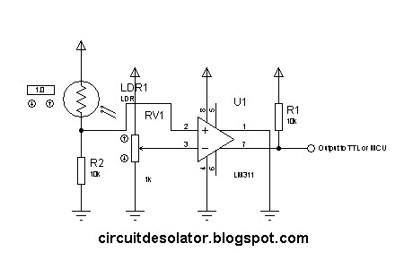
simple analog comparator
This is a common circuit block utilized in both digital and analog electronics. Its output depends on the relationship between its two input pins. One input is designated to provide the reference voltage, while the other is typically connected to...

simple magnitude comparator
In designing a logic circuit, it is often necessary to compare the values of two digital data inputs. Creating a custom magnitude comparator can lead to increased use of logic integrated circuits (ICs), as well as greater time and cost...
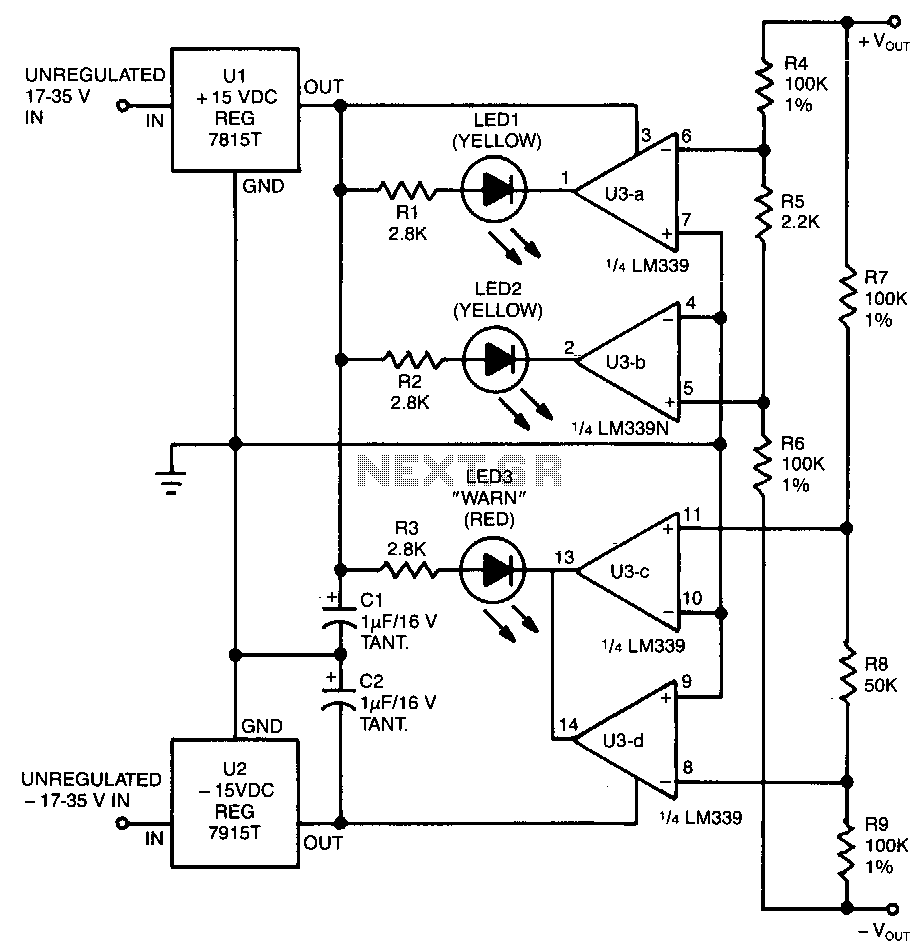
Power-supply-balance-indicator
This circuit utilizes two pairs of comparators from an LM339N quad comparator. One pair controls the yellow positive (+) and negative (-) indicators, while the other pair drives the red warning LED3. The circuit is powered by the unregulated section...
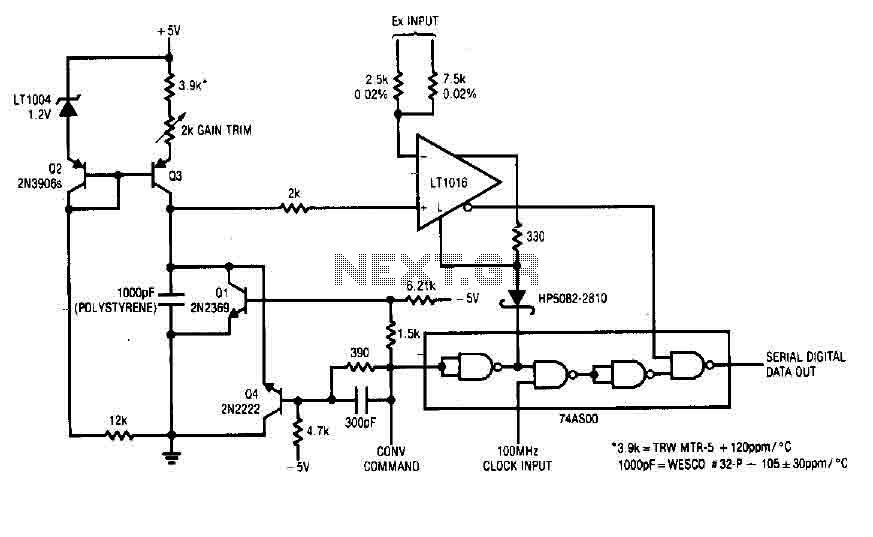
10 Bit A-D converter circuit
Each time a pulse is applied to the control input for conversion, Q1 resets the 1000 pF capacitor to 0 V. This resetting action takes 200 ns, after which the capacitor begins to charge linearly. In precisely 10 microseconds, it...

Null-detector
In this indicating comparator circuit, R2 sets the hysteresis. If the 741 saturates at ±12 V, the current in R1 will be approximately ±10 mA if a 0.1 V hysteresis is desired. More: Then 0.1 V/10 mA ~ 100.
The indicating...
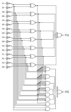
IC Magnitude Comparators
This Magnitude Comparator can be used to perform comparisons of two 8-bit binary or BCD words. The output provides both a P equals Q function and a P greater than Q function. A Magnitude Comparator is typically classified as standard...
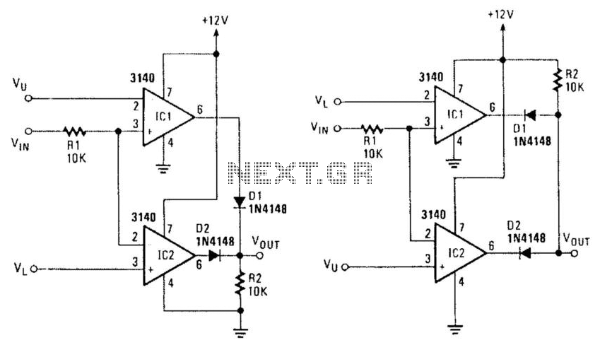
Window Comparators
In Figure 104-3(a), when the input voltage (Vin) is between the reference voltages (Vi and Vu), the output voltage (Vout) is low. If Vin exceeds the lower reference voltage (Vl), integrated circuit IC2 generates a low output. Additionally, if Vin...
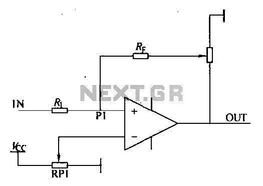
Loop comparator circuit
Environmental interference can affect the transfer switching, leading to the production of burrs in confidence disgrace. The switch position signal will control the computer system with the reliability of lanthanum burrs. The work has some impact. Glitches are typically addressed...