


16 bit Analogue to Digital Converter LTC1052
#analogue to digital converter
#LTC1052
#current balancing
#flip-flop
#current sink
#offset elimination
#precision measurement
#signal conversion
#circuit design
#electronic components
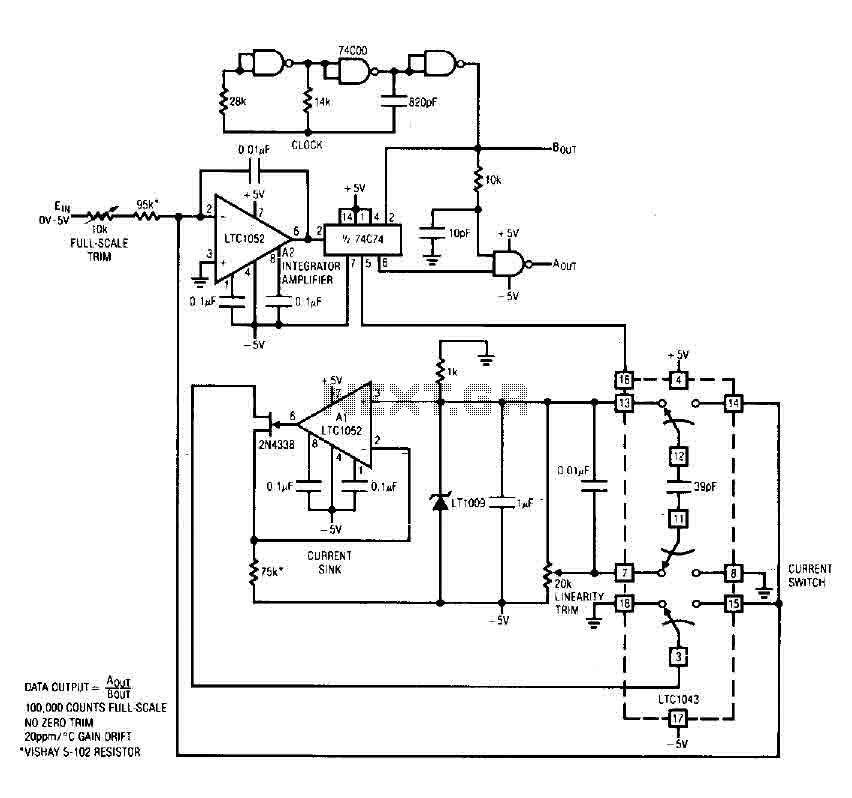
Description: The circuit is an analog-to-digital (A/D) converter that consists of an operational amplifier (A2), a flip-flop, several logic gates, and a current sink. It employs a current balancing technique. The LTC 1052 is utilized for stabilization, ensuring that the input voltage remains drift-free within a range of ±1°C to eliminate offset errors in the analog input.
The input voltage range for this A/D converter is specified to be from 0 to 5 volts.
This A/D converter circuit integrates several key components to achieve its functionality. The operational amplifier (A2) serves as a critical element in amplifying the analog signal before conversion. The choice of the LTC 1052 is particularly important due to its low drift characteristics, which help maintain accuracy in the conversion process by minimizing any offset errors that could arise from temperature fluctuations.
The flip-flop within the circuit plays a vital role in storing the converted digital output, ensuring that the data remains stable during the conversion process. Logic gates are incorporated to facilitate the necessary control logic for the conversion sequence, enabling the circuit to function effectively as an A/D converter.
The current sink is essential for providing a stable reference current, which aids in the current balancing technique employed in the circuit. This technique is crucial for achieving high precision in the conversion, as it ensures that the input signal is accurately represented in the digital domain.
Overall, the design of this A/D converter circuit is tailored to provide reliable and accurate conversion of analog signals within the specified input range, making it suitable for various applications in electronic systems requiring precise digital representation of analog inputs.The circuit here is a A/D converter, that consisting of A2, a flip-flop, some doors and a current sink, is based on a current balancing technique. Again, the stabilized LTC 1052 50 no drift of V input 1 ° C is necessary to eliminate the offset errors of aid.
Input has to be from 0-5V.
The input voltage range for this A/D converter is specified to be from 0 to 5 volts.
This A/D converter circuit integrates several key components to achieve its functionality. The operational amplifier (A2) serves as a critical element in amplifying the analog signal before conversion. The choice of the LTC 1052 is particularly important due to its low drift characteristics, which help maintain accuracy in the conversion process by minimizing any offset errors that could arise from temperature fluctuations.
The flip-flop within the circuit plays a vital role in storing the converted digital output, ensuring that the data remains stable during the conversion process. Logic gates are incorporated to facilitate the necessary control logic for the conversion sequence, enabling the circuit to function effectively as an A/D converter.
The current sink is essential for providing a stable reference current, which aids in the current balancing technique employed in the circuit. This technique is crucial for achieving high precision in the conversion, as it ensures that the input signal is accurately represented in the digital domain.
Overall, the design of this A/D converter circuit is tailored to provide reliable and accurate conversion of analog signals within the specified input range, making it suitable for various applications in electronic systems requiring precise digital representation of analog inputs.The circuit here is a A/D converter, that consisting of A2, a flip-flop, some doors and a current sink, is based on a current balancing technique. Again, the stabilized LTC 1052 50 no drift of V input 1 ° C is necessary to eliminate the offset errors of aid.
Input has to be from 0-5V.
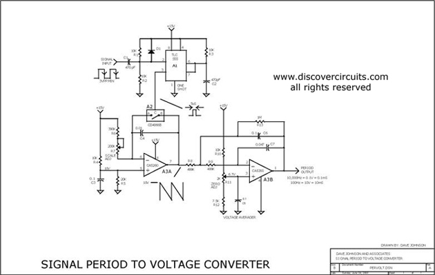
PULSE PERIOD TO VOLTAGE CONVERTER
This circuit is designed to convert a square wave input signal into a voltage output. The voltage produced is proportional to the time interval between the edges (period) of the signal, rather than its frequency. The operational range of the...
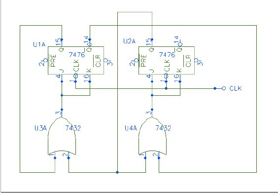
flipflop What happens when theres no specific input variable on a logic diagram using a JK flip flop
Q1 and Q2 form a table. On the left side, list the four possible states of Q1 and Q2; on the right side, write the values that Q1 and Q2 will assume after the next clock pulse. The table will...
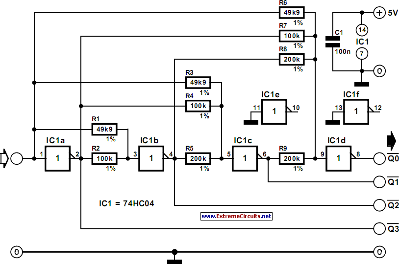
4-Bit Analogue to Digital Converter
The operation of the converter relies on the weighted addition and transfer of the analog input levels to the digital output levels. It comprises comparators and resistors. Although, theoretically, the number of bits is unlimited, each bit requires a comparator...
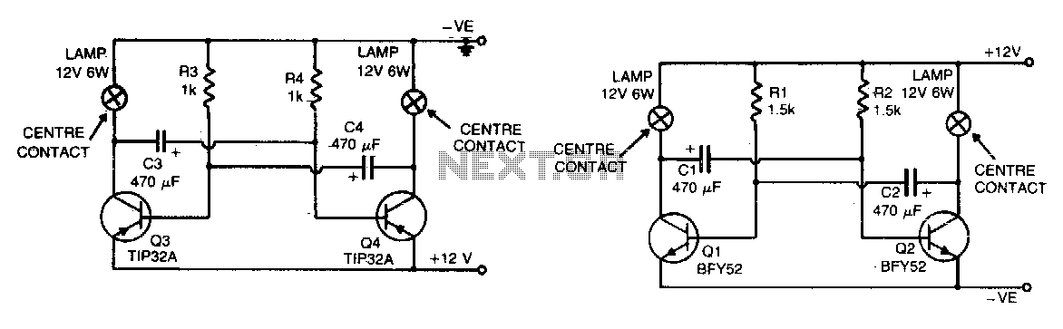
Flip-flop flasher
The flashing action is generated by a basic astable multivibrator configured to produce a flashing rate of approximately 60 flashes per minute for each lamp. The circuit designed for positive earth systems employs NPN transistors, while alternative configurations utilize PNP...
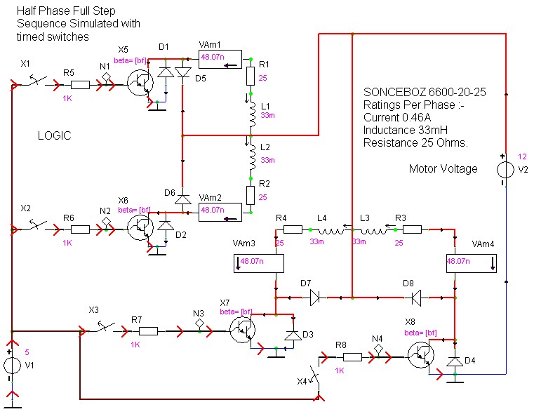
case stepper
Beige Bag Software has been offering affordable and innovative circuit design tools since 1990. B2 Spice provides schematics as well as analog, digital, and mixed-mode electronic circuit simulation. It integrates with EAGLE and CADSTAR PCB software.
B2 Spice is a powerful...
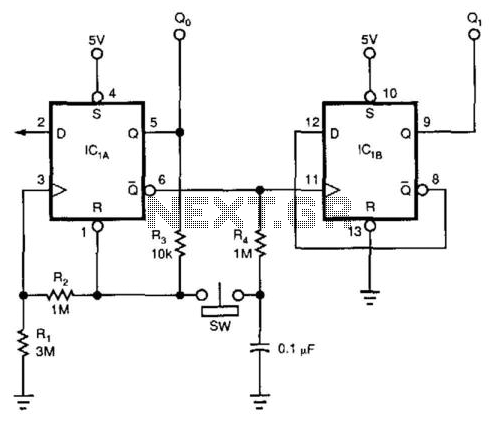
Flip-Flop Debouncer Switch
This circuit utilizes a 74HC74 flip-flop, although any CMOS variant of this component can be employed. IC1A functions as a true/complement buffer. Resistors R1 and R2 ensure that IC1A exits the reset state prior to the clock edge occurrence. Resistor...
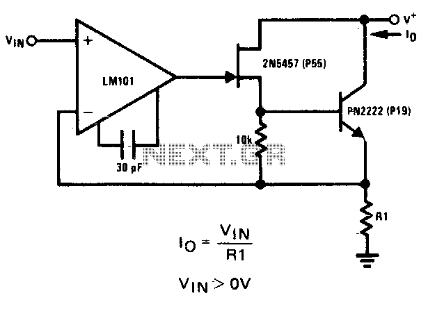
Precision current sink
The 2N5457 JFET and PN2222 bipolar transistor exhibit high output impedance. Employing Rl as a current sensing resistor to feedback into the LM101 operational amplifier yields significant loop gain for negative feedback, thereby improving the circuit's capability as a current...
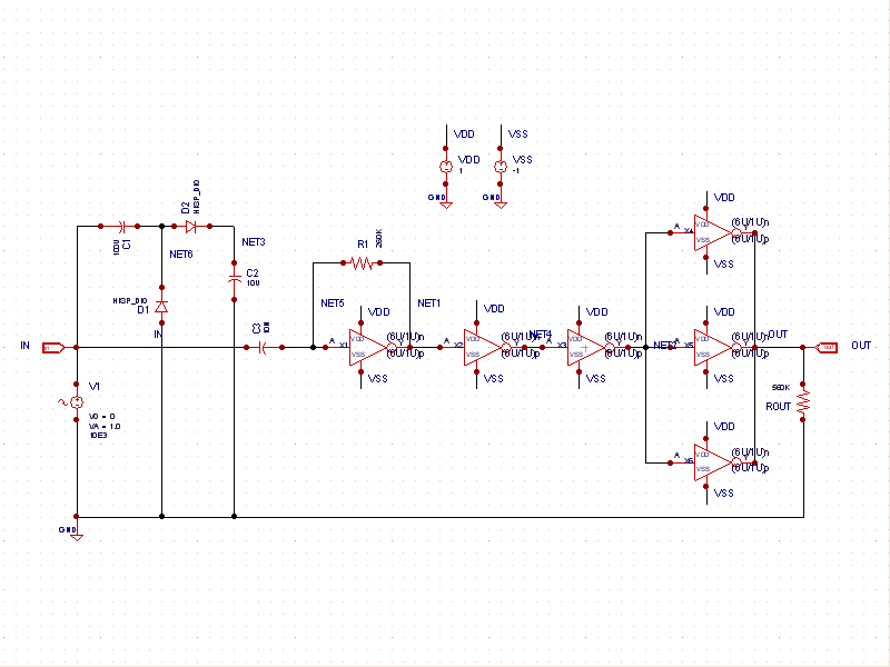
Sine to Square Wave Converter
This schematic example demonstrates a sinusoidal voltage input at a frequency of 10 kHz, which is converted to a square wave using an inverter-based circuit. The VDD and VSS rails are connected to +1V and -1V, respectively. The control file...
PULSE PERIOD TO VOLTAGE CONVERTER
This circuit is designed to convert a square wave input signal into a voltage output. The voltage produced is proportional to the time interval between the edges (period) of the signal, rather than its frequency. The operational range of the...