


Adjustable Attenuator for Oscilloscope
#attenuator
#oscilloscope
#FET buffer
#commutating capacitor
#input capacitance
#DC-10MHz
#1M ohm
#scale sensitivity
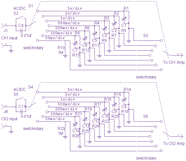
Description: The input attenuator uses a commutating capacitor to cancel the input capacitance of the FET buffer (see DC-10 MHz amp schematic). The commutating capacitors are absolutely necessary to cancel the effect of the input capacitance to the DC-10MHz amplifier. The theory of the commutating capacitors will not be discussed here. The input resistance is 1M ohm at all range settings. All resistances should be chosen to provide 1M ohms at any scale sensitivity. However the ratio of the resistances should also be chosen to provide the scale sensitivities shown below.
The described input attenuator circuit employs a commutating capacitor mechanism to effectively mitigate the input capacitance associated with the Field Effect Transistor (FET) buffer. This is particularly crucial for maintaining the performance of the DC-10 MHz amplifier, as excess input capacitance can adversely affect the frequency response and overall signal integrity.
In this circuit, the commutating capacitors are strategically implemented to ensure that they counterbalance the input capacitance, thereby stabilizing the input signal across the specified frequency range. The input resistance is maintained at a consistent level of 1 MΩ across all range settings, which is essential for ensuring that the circuit operates within the desired parameters regardless of the selected sensitivity scale.
The design mandates that all resistive components be selected to achieve this 1 MΩ input resistance, while also considering the ratios of these resistances. This ratio is critical as it determines the scale sensitivities, allowing the circuit to correctly attenuate the input signals according to the specified settings. Careful selection and arrangement of these resistors will enable the attenuator to provide accurate and reliable performance across its operational range.
Overall, the integration of commutating capacitors in conjunction with precisely chosen resistive elements forms a robust input attenuator design that is well-suited for applications requiring high-frequency signal processing while maintaining optimal input impedance characteristics.The input attenuator uses a commutating capacitor to cancel the input capacitance of the FET buffer (see DC-10 MHz amp schematic). The commutating capacitors are absolutely necessary to cancel the effect of the input capacitance to the DC-10MHz amplifier.
The theory of the commutating capacitors will not be discussed here. The input resistance is 1M ohm at all range settings. All resistances should be chosen to provide 1M ohms at any scale sensitivity. However the ratio of the resistances should also be chosen to provide the scale sensitivities shown below.
The described input attenuator circuit employs a commutating capacitor mechanism to effectively mitigate the input capacitance associated with the Field Effect Transistor (FET) buffer. This is particularly crucial for maintaining the performance of the DC-10 MHz amplifier, as excess input capacitance can adversely affect the frequency response and overall signal integrity.
In this circuit, the commutating capacitors are strategically implemented to ensure that they counterbalance the input capacitance, thereby stabilizing the input signal across the specified frequency range. The input resistance is maintained at a consistent level of 1 MΩ across all range settings, which is essential for ensuring that the circuit operates within the desired parameters regardless of the selected sensitivity scale.
The design mandates that all resistive components be selected to achieve this 1 MΩ input resistance, while also considering the ratios of these resistances. This ratio is critical as it determines the scale sensitivities, allowing the circuit to correctly attenuate the input signals according to the specified settings. Careful selection and arrangement of these resistors will enable the attenuator to provide accurate and reliable performance across its operational range.
Overall, the integration of commutating capacitors in conjunction with precisely chosen resistive elements forms a robust input attenuator design that is well-suited for applications requiring high-frequency signal processing while maintaining optimal input impedance characteristics.The input attenuator uses a commutating capacitor to cancel the input capacitance of the FET buffer (see DC-10 MHz amp schematic). The commutating capacitors are absolutely necessary to cancel the effect of the input capacitance to the DC-10MHz amplifier.
The theory of the commutating capacitors will not be discussed here. The input resistance is 1M ohm at all range settings. All resistances should be chosen to provide 1M ohms at any scale sensitivity. However the ratio of the resistances should also be chosen to provide the scale sensitivities shown below.
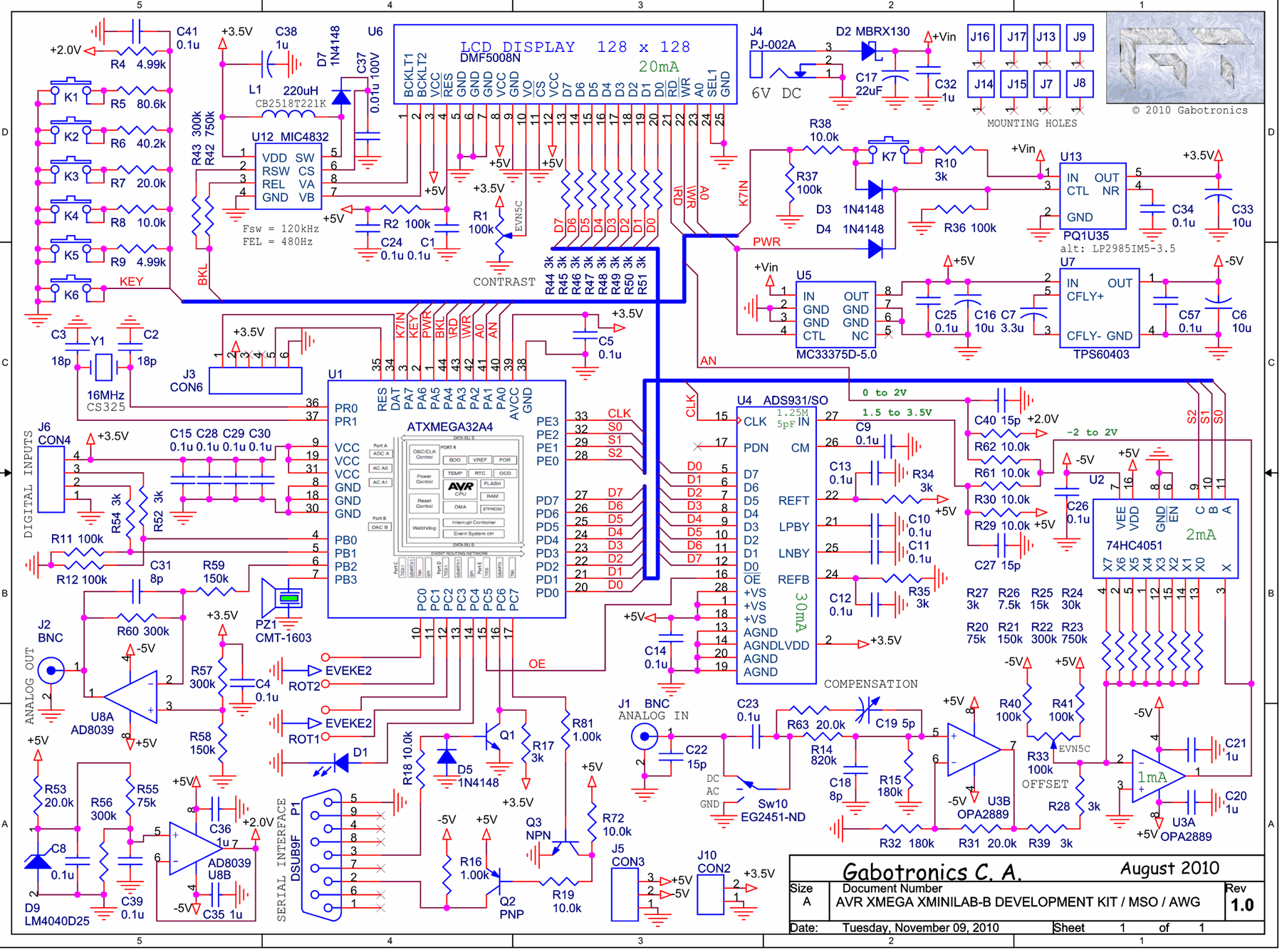
Oscilloscope Xminilab-B on the microcontroller Atmel AVR ATXMEGA32A4
The Xminilab-B oscilloscope is based on the Atmel AVR ATXMEGA32A4 microcontroller. It is designed as a debug board by the Gabotronis company, as noted on rlocman.ru.
The Xminilab-B oscilloscope features a compact and efficient design that leverages the capabilities of the...
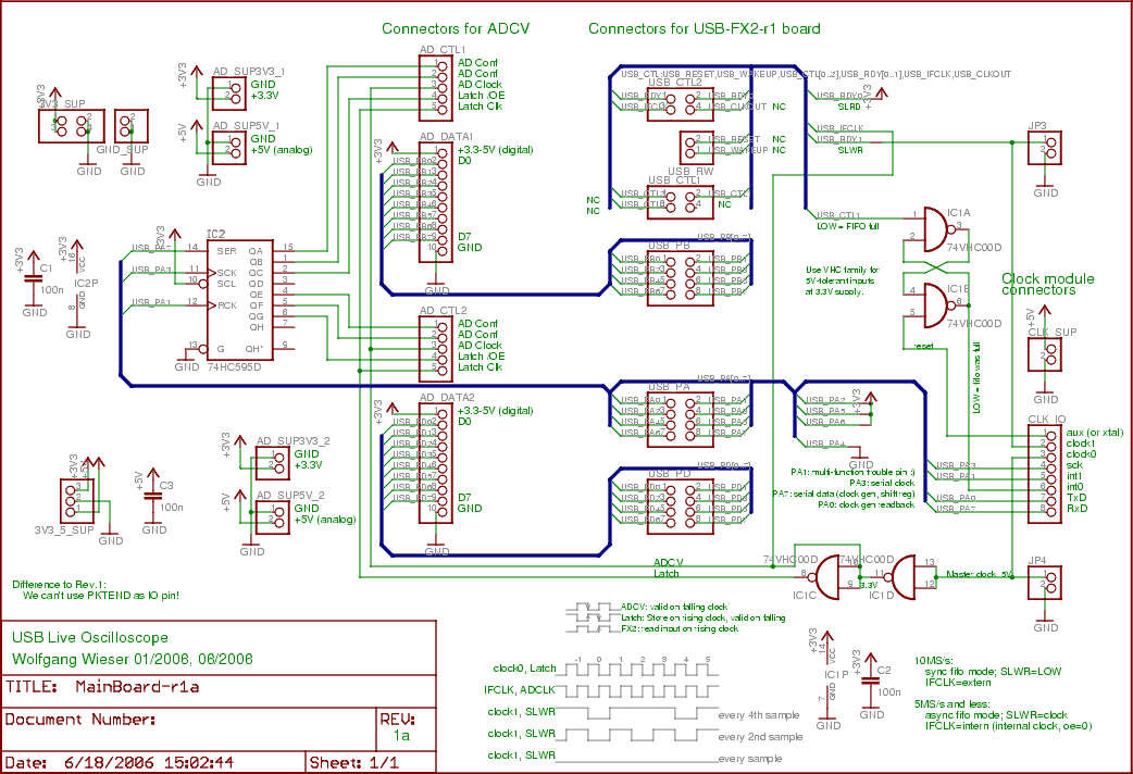
USB Live Oscilloscope: Main Board
The two input boards (ADCV or digital) are connected to AD_CTL1, AD_DATA1, AD_SUP5V_1, and AD_SUP3V3_1 for the first board, with the second board using the same connections but with a suffix of 2. To transfer sampling data, the 16 digital...
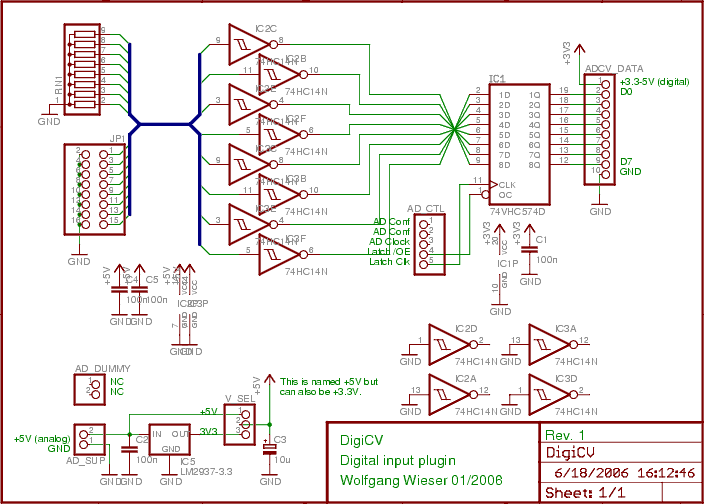
USB Live Oscilloscope: Digital Input Board
The digital input board features eight distinct digital inputs available on connector JP1. Each input is equipped with separate pull-down resistors (RN1, with a recommended value of 1 MΩ) and a Schmitt-trigger. To prevent damage from improper input voltages, HC14...
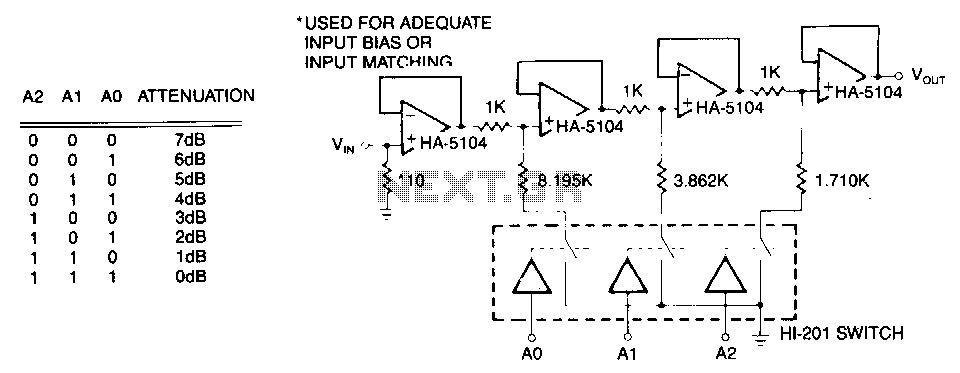
Digitally-programmable-attenuator
The first stage is a simple buffer used to isolate the signal source from the following attenuator stages. Each subsequent stage is preceded by a voltage divider formed by two resistors and a CMOS switch. When the CMOS switch for...
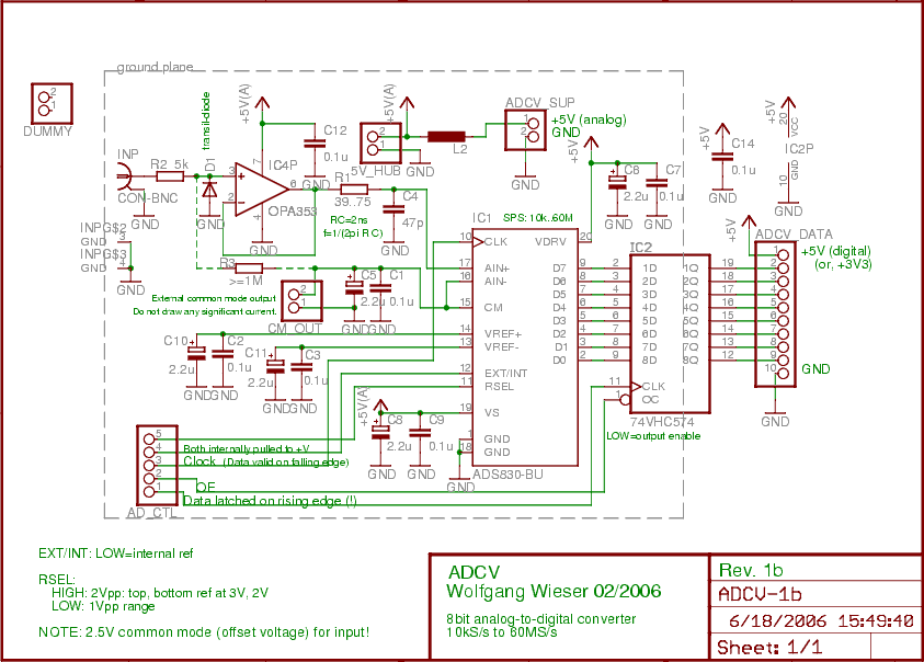
USB Live Oscilloscope: ADCV Board
The analog input is initially connected to a fast non-inverting buffer amplifier (OPA353) configured for unity gain, which safeguards the analog-to-digital converter from out-of-range voltages. The ADS830 is an economical 8-bit analog-to-digital converter that accommodates sampling clocks ranging from 10...
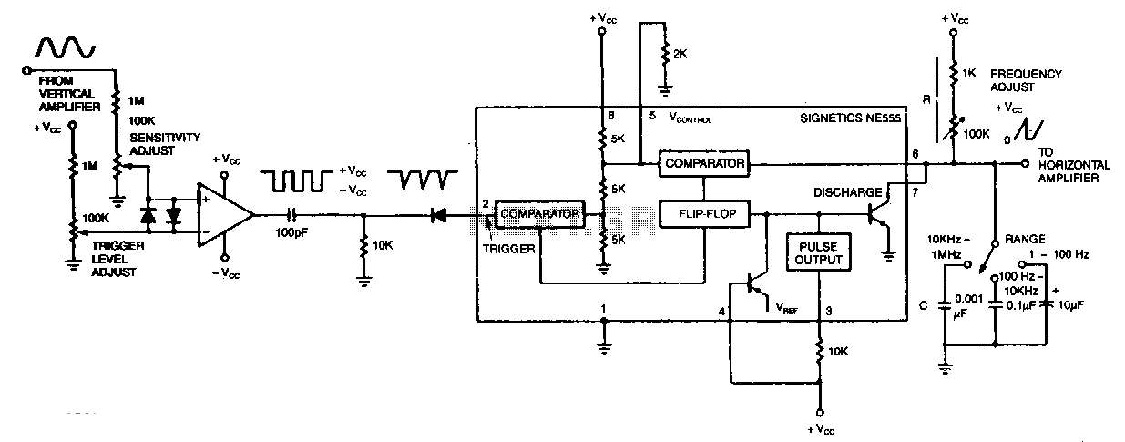
Oscilloscope triggered sweep circuit
The circuit's input operational amplifier triggers the timer, sets its flip-flop, and cuts off its discharge transistor, allowing capacitor C to charge. When the voltage across the capacitor reaches the timer's control voltage of 0.33 Vee, the flip-flop resets, and...
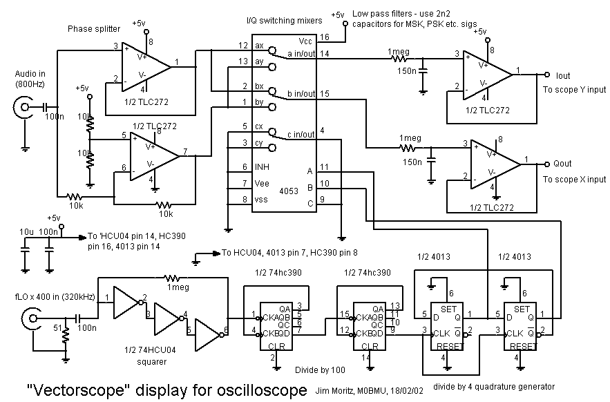
Phase indication by vectorscope
An oscilloscope capable of displaying in X/Y mode and a reference "LO" signal source are required. In-phase and quadrature reference square wave signals are generated using a divide-by-4, 2-bit ring counter with two D-type flip-flops. To utilize an RF generator...
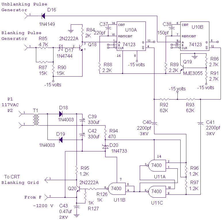
Blanking Circuit for Oscilloscope
This circuit blanks the CRT starting just before retrace begins. Since the CRT sits at a -1200 volt potential, the blanking circuit must also be based at -1200 volts. Note the capacitors, C40, C41, and C43 which allow the gates...
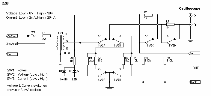
Component Signature for Oscilloscope
The general (and very basic) principle of operation is shown in Figure 1. The test signal is simply derived from the mains, and is a sinewave at 50 or 60Hz. In most locations, the sinewave will be distorted, but this...