


Linearized platinum resistance thermometer
#platinum resistance thermometer
#temperature measurement
#LT-1001
#precision
#calibration
#sensor circuit
#linearization
#accuracy
#voltage offset
#temperature drift
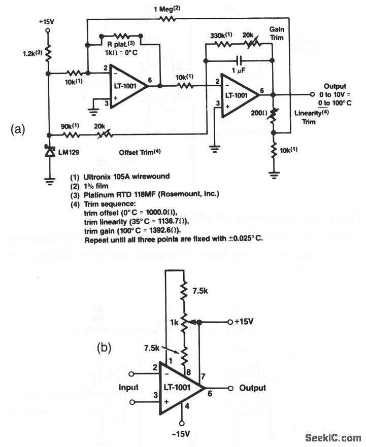
Description: This circuit demonstrates an accuracy of ±0.025 °C across a temperature range of 0 °C to 100 °C, based on the specified values. The LT-1001's input offset voltage and its temperature drift are permanently calibrated to a low level during wafer testing. If additional adjustment of the offset voltage (VOS) is required, the nulling circuit illustrated in Figure 10-4B can be utilized without adversely affecting the temperature drift. The offset circuit depicted in Figure 10-4B offers an approximate null range of ±100 V.
The described circuit utilizes the LT-1001 precision operational amplifier, which is known for its low input offset voltage and minimal drift with temperature variations. This makes it suitable for applications requiring high accuracy in temperature measurement. The calibration process at the wafer level ensures that the device is optimized for performance before it is integrated into the final application.
When adjustments to the input offset voltage are needed, the nulling circuit (Figure 10-4B) can be employed. This circuit is designed to provide a means of fine-tuning the offset without introducing additional drift, thereby maintaining the circuit's overall accuracy. The null range of approximately ±100 V indicates that significant adjustments can be made to accommodate variations in system requirements or component tolerances.
In practice, the implementation of this circuit involves careful consideration of the surrounding components, including resistors and capacitors that may be used in conjunction with the LT-1001. Proper layout and thermal management are essential to maintain accuracy and reliability, especially in environments where temperature fluctuations are expected. The circuit's design should also take into account power supply decoupling to minimize noise and improve performance.
Overall, this precision temperature measurement circuit exemplifies the integration of advanced electronic components to achieve high levels of accuracy and stability, making it suitable for a wide range of applications in industrial, medical, and scientific fields.With the values shown, this circuit has a ±0. 025 °C accuracy over 0 ° to 100 °C. The input offset voltage of the LT-1001, and its drift with temperature, are permanently trimmed at wafer test to a low level. However, if further adjustment of VOS is necessary, nulling with the circuit of Fig. 10-4B will not degrade drift with temperature. The Fig. 10-4B offset circuit has an approximate null range of ±100 V. o Raytheon U near Integrated a rcuts 1989, p. 4-45.
The described circuit utilizes the LT-1001 precision operational amplifier, which is known for its low input offset voltage and minimal drift with temperature variations. This makes it suitable for applications requiring high accuracy in temperature measurement. The calibration process at the wafer level ensures that the device is optimized for performance before it is integrated into the final application.
When adjustments to the input offset voltage are needed, the nulling circuit (Figure 10-4B) can be employed. This circuit is designed to provide a means of fine-tuning the offset without introducing additional drift, thereby maintaining the circuit's overall accuracy. The null range of approximately ±100 V indicates that significant adjustments can be made to accommodate variations in system requirements or component tolerances.
In practice, the implementation of this circuit involves careful consideration of the surrounding components, including resistors and capacitors that may be used in conjunction with the LT-1001. Proper layout and thermal management are essential to maintain accuracy and reliability, especially in environments where temperature fluctuations are expected. The circuit's design should also take into account power supply decoupling to minimize noise and improve performance.
Overall, this precision temperature measurement circuit exemplifies the integration of advanced electronic components to achieve high levels of accuracy and stability, making it suitable for a wide range of applications in industrial, medical, and scientific fields.With the values shown, this circuit has a ±0. 025 °C accuracy over 0 ° to 100 °C. The input offset voltage of the LT-1001, and its drift with temperature, are permanently trimmed at wafer test to a low level. However, if further adjustment of VOS is necessary, nulling with the circuit of Fig. 10-4B will not degrade drift with temperature. The Fig. 10-4B offset circuit has an approximate null range of ±100 V. o Raytheon U near Integrated a rcuts 1989, p. 4-45.
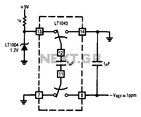
Precision-voltage-inverter
This circuit enables the inversion of a reference signal with an accuracy of 1 ppm. It features high input impedance and does not require any trimming.
The described circuit is designed to invert a reference voltage signal while maintaining a high...
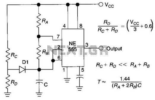
Precision Lf Oscillator Circuit
Using Rl, R7, and D1 to preset CI to one third of the supply voltage. This circuit avoids a longer first cycle period than subsequent cycles.
The circuit described involves the use of resistors Rl and R7 along with diode D1...
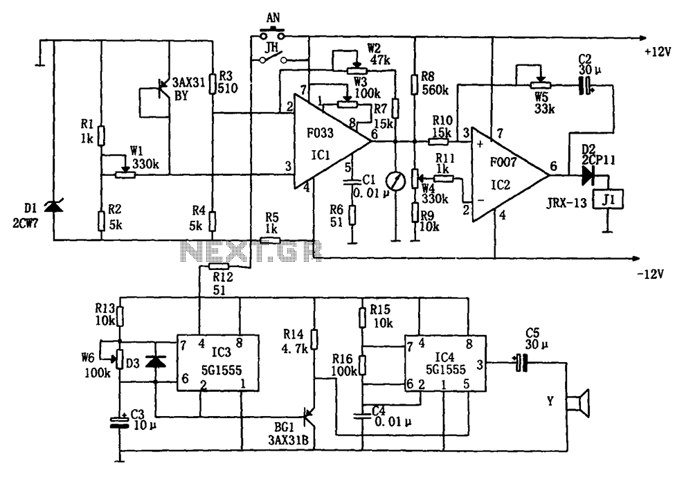
Treasury temperature measurement alarm circuit diagram F007 5G1555 F033
The temperature alarm circuit shown in the figure consists of an inverting amplifier (IC1), a comparison amplifier (IC2), a low-frequency multivibrator (IC3), a controllable oscillation frequency multivibrator (IC4), a bridge measurement network, a speaker (Y), and a power supply circuit....
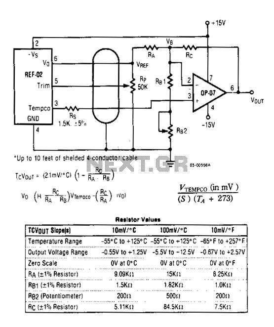
Temperature-measuring-add-on-for-dmm-digital-voltmeter
The DVM-to-temperature adapter is constructed around a single integrated circuit (IC), the National LM10. This micropower IC features a stable 0.2 V reference, a reference amplifier, and a general-purpose operational amplifier. The circuit is designed to operate within a linear...
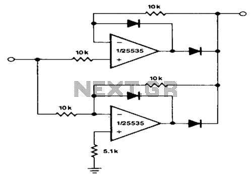
Precision-full-wave-rectifier
This circuit provides accurate full-wave rectification. The output impedance is low for both input polarities, and the errors are small at all signal levels. It is important to note that the output will not sink heavy currents, except for a...
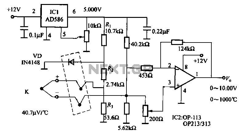
OP113 wide range of precision temperature measurement circuit
The circuit includes a K-type thermocouple cold junction compensation circuit, a precision 5.000V reference voltage source, and an OP113 operational amplifier. It is capable of measuring temperatures ranging from 0°C to 100°C with a resolution of 0.02°C. The OP113 is...
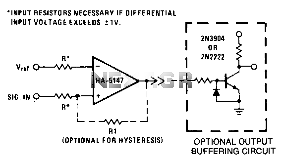
Precision-threshold-detector
This circuit requires low noise, stable offset voltages, high open-loop gain, and high speed. These requirements are fulfilled by the HA5147. Standard variations of this circuit can be easily implemented using the HA-5147. For instance, hysteresis can be introduced by...
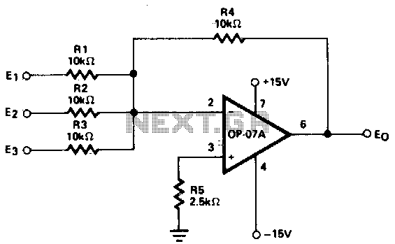
Adjustment-free precision summing amplifier
This circuit generates continuous outputs that depend on multiple input variables.
The circuit in question typically employs a combination of operational amplifiers (op-amps), resistors, and potentiometers to achieve its functionality. The outputs can be tailored based on the variations in...

Digital Remote Thermometer
This circuit is intended for precision centigrade temperature measurement, with a transmitter section converting to frequency the sensor's output voltage, which is proportional to the measured temperature. The output frequency bursts are conveyed into the mains supply cables. The receiver...