


Oscilloscope 4 Channel Adapter
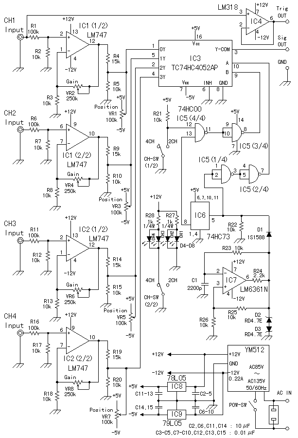
Description: The method goes by the switching method. Making it be possible to see four kinds of the input signals at the same time by switching them at the short period. In addition to the way of introducing here, there is a method which changes the input every period. In case of the method, the changing speed may be low-speed comparatively. The vertical position adjustment is making the direct current rise one above another with the output. (±5V) Because LM747 had the terminal for the offset control, I intended to use this. However, because the voltage change range was small, it wasn't possible to use for the justification. Originally, this terminal is not the terminal for the position adjustment. The way this time is the way that there is a little impossibility. When adjusting the position, the output voltage, too, has changed. It is possible to use if not making the top or bottom extremely. The signal vertical (the voltage axis) can be adjusted with VR1. But, that the oscilloscope to use can be displayed in the direct current is the condition. It is the circuit which does the switch of the four input signals. As the IC, it is using the thing for the switching of the analog signal. Because the power supply voltage of this IC is using ±5 V, it can handle the signal in the ±5 V range as the signal. According to the condition of the switch control line, the input signal of CH1-CH4 appears in the output. As for the figure on the left, the changing frequency is in the condition which isn't too fast to the frequency of the input signal. Because it is, the output signal (red) becomes the dotted line. Actually, if the input signal is lower sufficiently than the switching frequency, you can see the continued line. Because it wasn't possible to use the offset terminal, as the input amplifier, the operational amplifier can use TL084 with the housing of the four in the 1 package. Because pin connections are different, the pattern must be reformed. It is adjusting the mu factor of the amplifier with VR2. When VR2 is the smallest (the condition which connected the output of the amplifier and the negative input terminal), the mu factor of the amplifier becomes 1. (Noninverting Gain amplification) Because the circuit this time made R3=10K-ohm, VR2=250K-ohm, it is (1+VR2/R3)=26 times when maximizing VR2. Because it makes the input 1/10 by the resistance division, and 1/2 by R4 and R5. It doesn't become more than ±12 V. R4 and R5 are to drop the voltage of the output. This is because the IC for the switching which connects the output works by ±5 V. It breaks when connecting the output of the input amplifier directly. Because it is R4=15K-ohm, R5=10K-ohm, it is 10/(15+10)=1/2.5. When ±12 V are output from the input amplifier, the voltage which is gained by R5 becomes ±4.8 V. The way this time is not the way which is good because the noise occurs. When making the input signal 1/10, the output approaches the noise level. The amplifier has been amplified including the noise.
The circuit described employs a switching method to allow simultaneous observation of four distinct input signals by rapidly toggling between them. This is facilitated by an analog switch IC powered by a dual supply of ±5V, which is essential for handling input signals within this voltage range. The circuit includes a vertical position adjustment feature, which utilizes a variable resistor (VR1) to modify the vertical positioning of the signal on an oscilloscope, contingent upon the oscilloscope's ability to display DC signals.
The switching mechanism ensures that the selected input signal from channels CH1 to CH4 is routed to the output based on the control line state. The frequency of the switching action is designed to be sufficiently slower than the frequency of the input signals to maintain a clear representation of the output waveform. If the input signal frequency is significantly lower than the switching frequency, a continuous line will be observed on the oscilloscope rather than a dotted representation.
Due to the limitations of the LM747 offset terminal, the circuit utilizes a TL084 operational amplifier, which is advantageous for its quad configuration, allowing for multiple amplifiers in a single package. The gain of the amplifier is adjustable via another variable resistor (VR2), with a minimum gain of 1 when VR2 is at its lowest setting, and a maximum gain of 26 when fully adjusted. The input signal is attenuated to one-tenth its original value through a resistor divider configuration, followed by further attenuation by resistors R4 and R5, ensuring that the output does not exceed ±12V, which is critical to prevent damage to the switching IC.
Resistors R4 (15K-ohm) and R5 (10K-ohm) serve to further reduce the output voltage to a safe level compatible with the switching IC. The calculated output from the input amplifier, when set to ±12V, results in an output voltage of approximately ±4.8V after passing through R5. However, the design is noted to have noise issues, particularly when the input signal is significantly attenuated, as the amplified output may approach the noise floor, impacting the signal integrity.The method goes by the switching method. Making it be possible to see four kinds of the input signals at the same time by switching them at the short period. In addition to the way of introducing here, there is a method which changes the input every period. In case of the method, the changing speed may be low-speed comparatively. The vertical position adjustment is making the direct current rise one above another with the output.(±5V) Because LM747 had the terminal for the offset control, I intended to use this.
However, because the voltage change range was small, it wasn't possible to use for the justification. Originally, this terminal is not the terminal for the position adjustment. The way this time is the way that there is a little impossibility. When adjusting the position, the output voltage, too, has changed. It is possible to use if not making the top or bottom extremely. The signal vertical (the voltage axis) can be adjusted with VR1. But, that the oscilloscope to use can be displayed in the direct current is the condition. It is the circuit which does the switch of the four input signals. As the IC, it is using the thing for the switching of the analog signal. Because the power supply voltage of this IC is using ±5 V, it can handle the signal in the ±5 V range as the signal. According to the condition of the switch control line, the input signal of CH1-CH4 appears in the output.
As for the figure on the left, the changing frequency is in the condition which isn't too fast to the frequency of the input signal. Because it is, the output signal (red) becomes the dotted line. Actually, if the input signal is lower sufficiently than the switching frequency, you can see the continued line.
Because it wasn't possible to use the offset terminal, as the input amplifier, the operational amplifier can use TL084 with the housing of the four in the 1 package. Because pin connections are different, the pattern must be reformed. It is adjusting the mu factor of the amplifier with VR2. When VR2 is the smallest (the condition which connected the output of the amplifier and the negative input terminal), the mu factor of the amplifier becomes 1.(Noninverting Gain amplification) Because the circuit this time made R3=10K-ohm, VR2=250K-ohm, it is (1+VR2/R3)=26 times when maximizing VR2.
Because it makes the input 1/10 by the resistance division, and 1/2 by R4 and R5. It doesn't become more than ±12 V . R4 and R5 are to drop the voltage of the output. This is because the IC for the switching which connects the output works by ±5 V. It breaks when connecting the output of the input amplifier directly. Because it is R4=15K-ohm, R5=10K-ohm, it is 10/(15+10)=1/2.5. When ±12 V are output from the input amplifier, the voltage which is gained by R5 becomes ±4.8 V. The way this time is not the way which is good because the noise occurs. When making the input signal 1/10, the output approaches the noise level. The amplifier has been amplified including the noise.
The circuit described employs a switching method to allow simultaneous observation of four distinct input signals by rapidly toggling between them. This is facilitated by an analog switch IC powered by a dual supply of ±5V, which is essential for handling input signals within this voltage range. The circuit includes a vertical position adjustment feature, which utilizes a variable resistor (VR1) to modify the vertical positioning of the signal on an oscilloscope, contingent upon the oscilloscope's ability to display DC signals.
The switching mechanism ensures that the selected input signal from channels CH1 to CH4 is routed to the output based on the control line state. The frequency of the switching action is designed to be sufficiently slower than the frequency of the input signals to maintain a clear representation of the output waveform. If the input signal frequency is significantly lower than the switching frequency, a continuous line will be observed on the oscilloscope rather than a dotted representation.
Due to the limitations of the LM747 offset terminal, the circuit utilizes a TL084 operational amplifier, which is advantageous for its quad configuration, allowing for multiple amplifiers in a single package. The gain of the amplifier is adjustable via another variable resistor (VR2), with a minimum gain of 1 when VR2 is at its lowest setting, and a maximum gain of 26 when fully adjusted. The input signal is attenuated to one-tenth its original value through a resistor divider configuration, followed by further attenuation by resistors R4 and R5, ensuring that the output does not exceed ±12V, which is critical to prevent damage to the switching IC.
Resistors R4 (15K-ohm) and R5 (10K-ohm) serve to further reduce the output voltage to a safe level compatible with the switching IC. The calculated output from the input amplifier, when set to ±12V, results in an output voltage of approximately ±4.8V after passing through R5. However, the design is noted to have noise issues, particularly when the input signal is significantly attenuated, as the amplified output may approach the noise floor, impacting the signal integrity.The method goes by the switching method. Making it be possible to see four kinds of the input signals at the same time by switching them at the short period. In addition to the way of introducing here, there is a method which changes the input every period. In case of the method, the changing speed may be low-speed comparatively. The vertical position adjustment is making the direct current rise one above another with the output.(±5V) Because LM747 had the terminal for the offset control, I intended to use this.
However, because the voltage change range was small, it wasn't possible to use for the justification. Originally, this terminal is not the terminal for the position adjustment. The way this time is the way that there is a little impossibility. When adjusting the position, the output voltage, too, has changed. It is possible to use if not making the top or bottom extremely. The signal vertical (the voltage axis) can be adjusted with VR1. But, that the oscilloscope to use can be displayed in the direct current is the condition. It is the circuit which does the switch of the four input signals. As the IC, it is using the thing for the switching of the analog signal. Because the power supply voltage of this IC is using ±5 V, it can handle the signal in the ±5 V range as the signal. According to the condition of the switch control line, the input signal of CH1-CH4 appears in the output.
As for the figure on the left, the changing frequency is in the condition which isn't too fast to the frequency of the input signal. Because it is, the output signal (red) becomes the dotted line. Actually, if the input signal is lower sufficiently than the switching frequency, you can see the continued line.
Because it wasn't possible to use the offset terminal, as the input amplifier, the operational amplifier can use TL084 with the housing of the four in the 1 package. Because pin connections are different, the pattern must be reformed. It is adjusting the mu factor of the amplifier with VR2. When VR2 is the smallest (the condition which connected the output of the amplifier and the negative input terminal), the mu factor of the amplifier becomes 1.(Noninverting Gain amplification) Because the circuit this time made R3=10K-ohm, VR2=250K-ohm, it is (1+VR2/R3)=26 times when maximizing VR2.
Because it makes the input 1/10 by the resistance division, and 1/2 by R4 and R5. It doesn't become more than ±12 V . R4 and R5 are to drop the voltage of the output. This is because the IC for the switching which connects the output works by ±5 V. It breaks when connecting the output of the input amplifier directly. Because it is R4=15K-ohm, R5=10K-ohm, it is 10/(15+10)=1/2.5. When ±12 V are output from the input amplifier, the voltage which is gained by R5 becomes ±4.8 V. The way this time is not the way which is good because the noise occurs. When making the input signal 1/10, the output approaches the noise level. The amplifier has been amplified including the noise.
Radio Buttons Using Push On Switch Latching Circuit
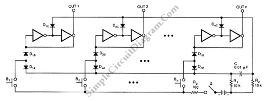
This is a switching circuit that provides a latching mechanism to create a set of radio buttons using push buttons. This circuit consists of an interlocking circuit.
The switching circuit operates on the principle of latching, allowing multiple push buttons to...
Phase indication by vectorscope
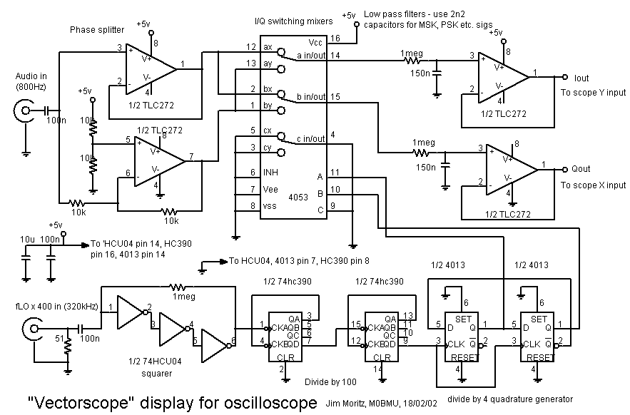
An oscilloscope capable of displaying in X/Y mode and a reference "LO" signal source are required. In-phase and quadrature reference square wave signals are generated using a divide-by-4, 2-bit ring counter with two D-type flip-flops. To utilize an RF generator...
Blanking Circuit for Oscilloscope
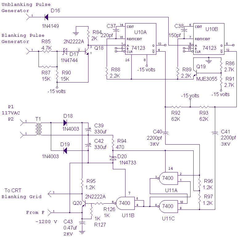
This circuit blanks the CRT starting just before retrace begins. Since the CRT sits at a -1200 volt potential, the blanking circuit must also be based at -1200 volts. Note the capacitors, C40, C41, and C43 which allow the gates...
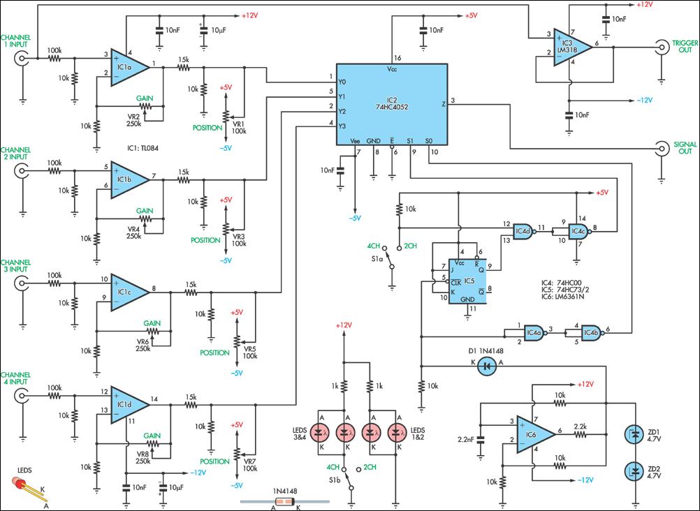
Four-Channel Oscilloscope Adaptor
This circuit allows for the simultaneous display of four signals using a single channel of an oscilloscope. It sequentially switches each input to the output with some signal processing in between. It is designed for low-frequency signal measurements and does...
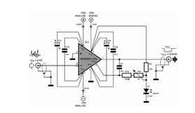
Spike Detector For Oscilloscopes
Dynamic flip-flops disregard input pulses that are shorter than 40 ns or do not conform to TTL voltage levels. Consequently, TTL flip-flops are not well-suited for certain applications.
Dynamic flip-flops are a specific type of sequential logic circuit that utilize dynamic...
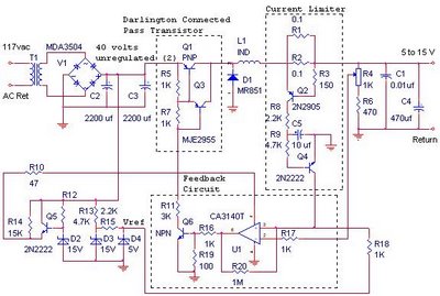
Schematics power supply switching PCB
The switching power supply provides 12 volts at a maximum of 10 amps, utilizing a discrete transistor regulator with an operational amplifier acting as a comparator in the feedback circuit. The schematic does not depict the front panel power-on indicator....
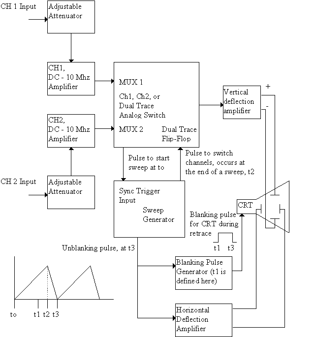
Dual-trace, triggered oscilloscope
This site contains public-domain schematics for a dual-trace, triggered oscilloscope, and some theory. Click on the topic in the table below to see the schematic for that block. I designed and built this oscilloscope in 1986 using the chassis of...
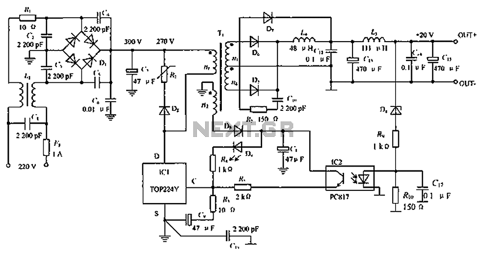
Low-noise switching power supply schematic circuit diagram
The circuit depicted in the figure is designed to achieve a higher power output by modifying specific components. On the left side of the figure, components R1, L1, D1, and capacitors C1 to C7 form a conventional filtering and rectifying...
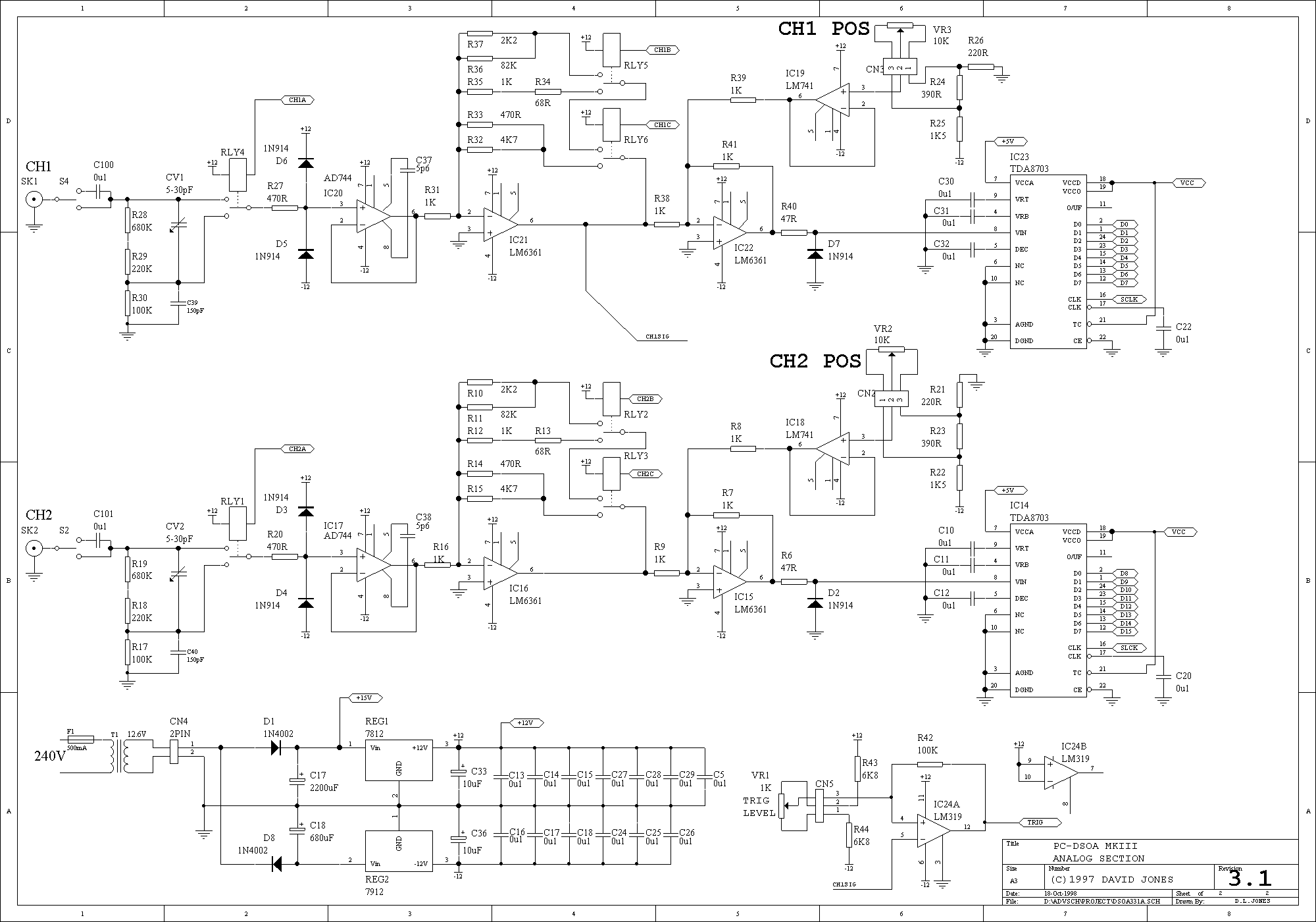
Digital Storage Oscilloscope Adapter
A follow up Mk2 version described by EA's Jim Rowe in the May/June/July 94 issues of EA improved on the original with calibrated time and vertical scales, and extra triggering features. This design proved even more popular than the first,...