


Radiation Detector and Meter DT-590A/PDR-56F Scintillation Probe
#radiation detector
#scintillation probe
#high-voltage power supply
#inverter
#schematic diagram
#JKL BXA-12579
#cold-cathode fluorescent lamps
#rectifier
#voltage conversion
#home-built circuit
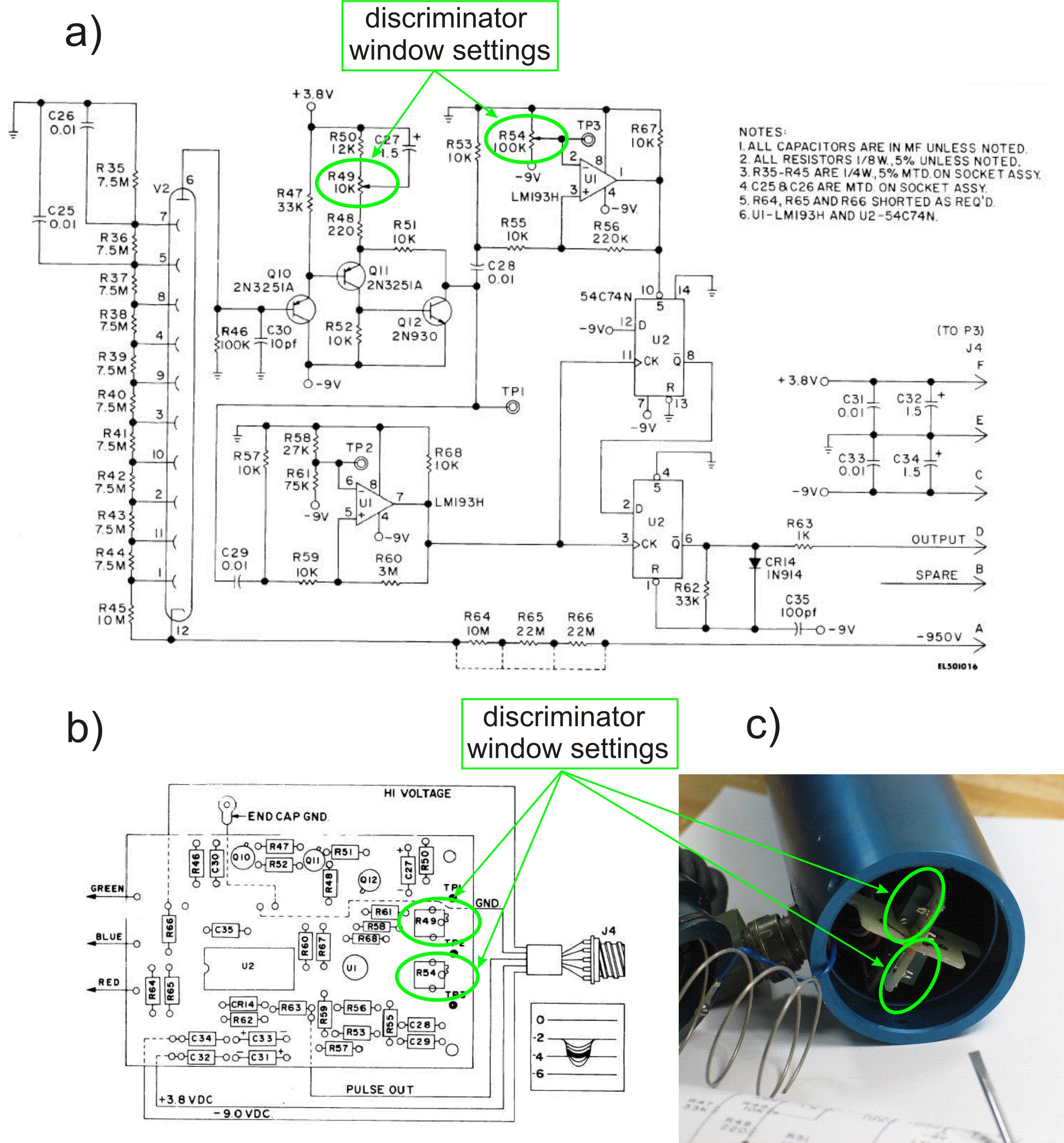
Description: This PDF file presents the schematic diagram of a custom-built circuit designed to drive the PDR-56 probe. A JKL BXA-12579 inverter, typically used for powering cold-cathode fluorescent lamps, serves as the high-voltage power supply. The BXA-12579 generates 1,500 VAC RMS from a 12 VDC input. The AC output is directly tapped from the transformer's secondary and rectified by D1, a high-voltage diode rated at 20 kV and 0.5 A. The rectified signal is filtered using capacitors C1, C2, and resistor R1. A voltage of -950 VDC, required for the operation of the photomultiplier tube within the PFR-56 probe, is regulated by a series of Zener diodes (D2 to D9). An isolated DKE 10A-05 DC/DC converter generates -9 V, while +3.8 V is derived from the 12 VDC input via a 5 V linear regulator (U1), with its output voltage reduced by two series diodes (D11 and D12). The signal input circuit is based on the military DT-590A/PDR-56 radiac meter, as detailed in the US Army Technical Manual TM 11-6665-245-34. In this section, transistors Q1, Q2, and Q3 form a discriminator and buffer-inverter circuit that determines the level of incoming pulses, providing a positive-going pulse for U2. Initially, with no signal (a positive pulse from the buffer-inverter circuit Q3), both inputs to NOR gate U2A are low, resulting in a high output and conduction of transistor Q4. A positive pulse from Q3 activates the circuit. When pin 1 of U2A goes high, its output switches to low. This voltage change is coupled directly to the base of Q4 through timing capacitor C10. Consequently, Q4 is cut off, causing its collector to go high, which holds the output of U2A low. This state persists until timing capacitor C10 discharges through resistor R10 sufficiently to allow Q4 to turn on, reverting pin 2 of U2A to a low state. This results in pin 3 of U2A first transitioning low due to the inverter-buffer input pulse and then remaining low until the timing capacitor discharges, generating a negative-going pulse at the inputs of U2B through U2D. The outputs from inverters U2B and U2C are connected to a piezo speaker to produce a click for each detection by the probe. Additionally, the output of U2D can be routed to a counter, small audio amplifier, or other instruments. The circuit within the probe is designed as a single-channel counter, factory-tuned to detect only scintillation pulses from Pu-239 gamma rays. It is recommended to open the single-channel window fully to enhance the probe's sensitivity across a broader range of gamma energies. The accompanying image illustrates the trimmers inside the probe that require re-adjustment.
The circuit described integrates multiple components to achieve high-voltage generation and precise signal processing for radiation detection. The JKL BXA-12579 inverter is critical in providing the necessary high voltage, while the rectification and filtering stages ensure a stable DC output for further processing. The use of Zener diodes for voltage regulation ensures that the delicate photomultiplier tube operates within its required parameters, enhancing the reliability of the detection system.
The signal processing section, utilizing a combination of transistors and NOR gates, allows for effective pulse discrimination and amplification. The design emphasizes the importance of timing and signal integrity, with careful consideration given to the interaction between the timing capacitor and the associated resistors. This ensures that the circuit can accurately respond to incoming radiation pulses, generating audible and visual feedback through the piezo speaker and potential output to other monitoring equipment.
The single-channel design of the probe, optimized for detecting specific gamma radiation, highlights the specialized nature of this application. Adjustments to the internal trimmers provide flexibility for calibration, ensuring that the probe can be fine-tuned for varying environmental conditions or specific detection requirements. This comprehensive approach to circuit design ensures effective radiation detection while maintaining user accessibility for adjustments and maintenance.This pdf file shows the schematic diagram of my home-built circuit to drive the PDR-56 probe. A JKL BXA-12579 inverter commonly used to drive cold-cathode fluorescent lamps is used as the high-voltage power supply. The BXA-12579 produces 1, 500 VACRMS for a 12 VDC input. The AC output is tapped straight from the transformer`s secondary and rectifie d by D1, a high-voltage diode rated at 20 kV and 0. 5 A. The rectified signal is filtered by C1, R1 and C2. -950 VDC for operation of the photomultiplier tube inside the PFR-56 probe are regulated by a series of Zener diodes (D2 D9). -9 V are generated by an isolated DKE 10A-05 DC/DC converter, and +3. 8 V are derived from the 12VDC input by a 3-pin 5 V linear regulator (U1) with its output voltage dropped by 2 series diodes (D11 and D12).
The signal input circuit is based directly on the military DT-590A/PDR-56 radiac meter as described in US Army Technical Manual TM 11-6665-245-34. In this part of the circuit, Q1, Q2 and Q3 form a discriminator and buffer-inverter circuit that determines the level of incoming pulses which are measured and provides a positive going pulse for use by U2.
Prior to any signal (positive pulse from the buffer inverter circuit Q3), the inputs to NOR gate U2A are both low, the output is high and transistor Q4 is conducting. A positive going pulse from Q3 starts the circuit into operation. When pin 1, U2A, goes high, its output goes low. The voltage change is coupled directly to the base of Q4 through timing capacitor C10. Q4 is then cut off and its collector goes high holding the output of U2A low. This condition holds until timing capacitor C10 discharges through resistor R10 enough to allow Q4 to turn on, causing pin 2 of U2A to revert to a low condition.
This action results in pin 3, U2A, first going low as the result of the inverter-buffer input pulse and then staying low until the timing capacitor discharges forming a negative going pulse on the inputs of U2B through U2D. Outputs from inverters U2B and U2C are tied together and connected to a piezo speaker to produce a click for each detection by the probe.
In addition, the output of U2D can be routed to a counter, small audio amplifier or other instrument. The circuit inside the probe is built as a single-channel counter, and is factory-tuned to detect only scintillation pulses from the Pu-239 gamma rays.
Thus, you shouldopen the single-channel window all the way tomake the probe sensitive to a much wider range of gamma energies. The following picture shows the trimmers inside the probe that need to be re-adjusted:
The circuit described integrates multiple components to achieve high-voltage generation and precise signal processing for radiation detection. The JKL BXA-12579 inverter is critical in providing the necessary high voltage, while the rectification and filtering stages ensure a stable DC output for further processing. The use of Zener diodes for voltage regulation ensures that the delicate photomultiplier tube operates within its required parameters, enhancing the reliability of the detection system.
The signal processing section, utilizing a combination of transistors and NOR gates, allows for effective pulse discrimination and amplification. The design emphasizes the importance of timing and signal integrity, with careful consideration given to the interaction between the timing capacitor and the associated resistors. This ensures that the circuit can accurately respond to incoming radiation pulses, generating audible and visual feedback through the piezo speaker and potential output to other monitoring equipment.
The single-channel design of the probe, optimized for detecting specific gamma radiation, highlights the specialized nature of this application. Adjustments to the internal trimmers provide flexibility for calibration, ensuring that the probe can be fine-tuned for varying environmental conditions or specific detection requirements. This comprehensive approach to circuit design ensures effective radiation detection while maintaining user accessibility for adjustments and maintenance.This pdf file shows the schematic diagram of my home-built circuit to drive the PDR-56 probe. A JKL BXA-12579 inverter commonly used to drive cold-cathode fluorescent lamps is used as the high-voltage power supply. The BXA-12579 produces 1, 500 VACRMS for a 12 VDC input. The AC output is tapped straight from the transformer`s secondary and rectifie d by D1, a high-voltage diode rated at 20 kV and 0. 5 A. The rectified signal is filtered by C1, R1 and C2. -950 VDC for operation of the photomultiplier tube inside the PFR-56 probe are regulated by a series of Zener diodes (D2 D9). -9 V are generated by an isolated DKE 10A-05 DC/DC converter, and +3. 8 V are derived from the 12VDC input by a 3-pin 5 V linear regulator (U1) with its output voltage dropped by 2 series diodes (D11 and D12).
The signal input circuit is based directly on the military DT-590A/PDR-56 radiac meter as described in US Army Technical Manual TM 11-6665-245-34. In this part of the circuit, Q1, Q2 and Q3 form a discriminator and buffer-inverter circuit that determines the level of incoming pulses which are measured and provides a positive going pulse for use by U2.
Prior to any signal (positive pulse from the buffer inverter circuit Q3), the inputs to NOR gate U2A are both low, the output is high and transistor Q4 is conducting. A positive going pulse from Q3 starts the circuit into operation. When pin 1, U2A, goes high, its output goes low. The voltage change is coupled directly to the base of Q4 through timing capacitor C10. Q4 is then cut off and its collector goes high holding the output of U2A low. This condition holds until timing capacitor C10 discharges through resistor R10 enough to allow Q4 to turn on, causing pin 2 of U2A to revert to a low condition.
This action results in pin 3, U2A, first going low as the result of the inverter-buffer input pulse and then staying low until the timing capacitor discharges forming a negative going pulse on the inputs of U2B through U2D. Outputs from inverters U2B and U2C are tied together and connected to a piezo speaker to produce a click for each detection by the probe.
In addition, the output of U2D can be routed to a counter, small audio amplifier or other instrument. The circuit inside the probe is built as a single-channel counter, and is factory-tuned to detect only scintillation pulses from the Pu-239 gamma rays.
Thus, you shouldopen the single-channel window all the way tomake the probe sensitive to a much wider range of gamma energies. The following picture shows the trimmers inside the probe that need to be re-adjusted:
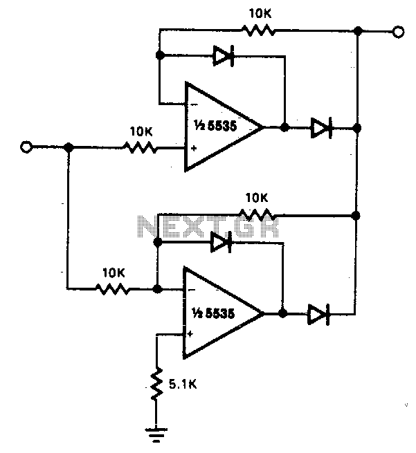
Precision full wave rectifier
The circuit facilitates precise full-wave rectification. It exhibits low output impedance for both input polarities, and the error rates remain minimal across all signal levels. It is important to note that the output will not be capable of sinking significant...
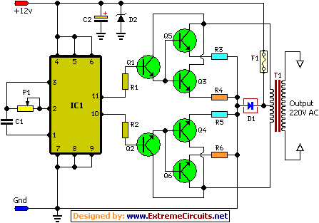
100w inverter circuit schematic
This document describes a 100 Watt inverter circuit that utilizes a minimal number of components. The circuit employs the CD 4047 integrated circuit (IC) from Texas Instruments to generate 100 Hz pulses, along with four 2N3055 transistors that drive the...
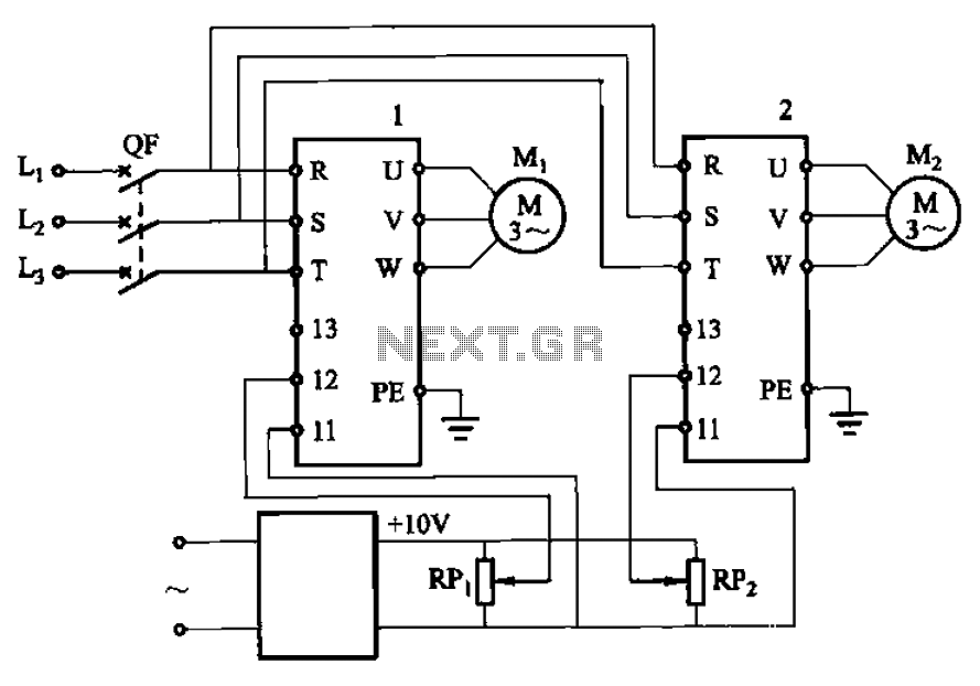
Two inverter controlled synchronous motor of the second circuit
Adjust the potentiometers RPi and RPz to modify the speed of two motors.
The circuit utilizes two potentiometers, designated as RPi and RPz, to control the speed of two separate motors. Each potentiometer is connected in a voltage divider configuration, enabling...
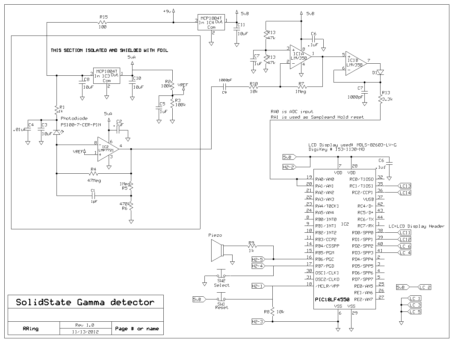
Solid State Radiation Detector with LCD Complete
A PIC microcontroller and an LCD have been integrated into a basic radiation detector, enabling the display of total counts over a 24-hour period or counts per second, as well as the relative gamma strike energy level. The energy level...
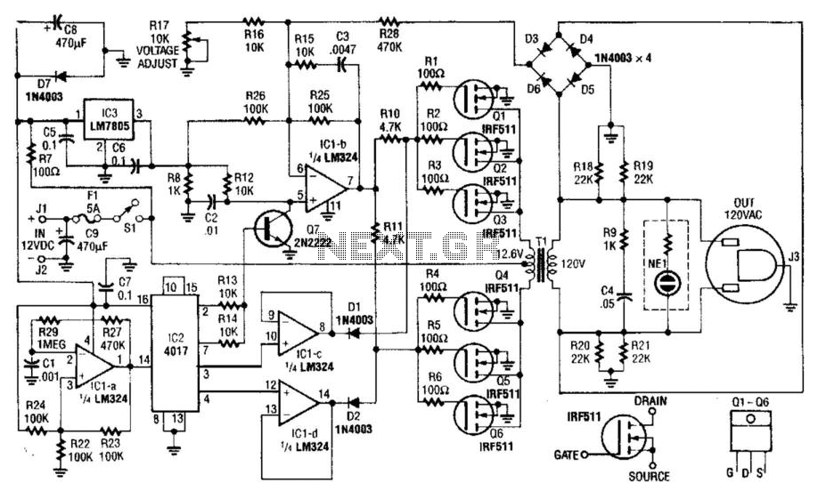
40W 120Vac Inverter
This inverter employs a 12.6-V to 120-V transformer to generate a quasi-sine wave that matches the rms and peak voltage of a pure sine wave. Components Q1 to Q6 require heatsinking, and a 1.5" x 4" aluminum heatsink was utilized...
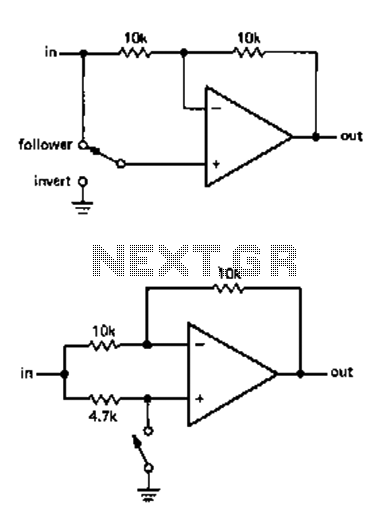
Optional Flip inverter circuit
The circuit allows for the reversal or flipping of switch amplification without inversion. The voltage gain is dependent on the position of the switch, which can be either +1 or -1. There are two versions of the circuit, A and...
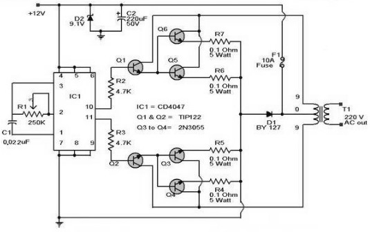
100w inverter circuit 12vdc to 220vac
A 12 V car battery can be utilized as the 12 V input power source. The potentiometer R1 can be adjusted to achieve a 50 Hz output frequency. It is recommended to use a 10 A fuse in series with...
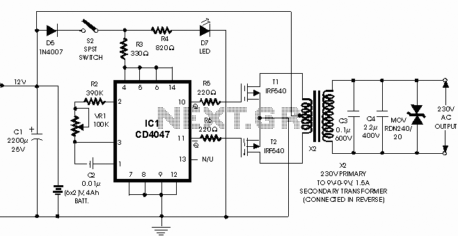
100Watt Inverter 24VDC to 220VAC II
This is a 100-watt inverter circuit diagram. It is built using the IC CD4047 and the MOSFET IRF540. This inverter has the capability to supply electronic devices that require 220VAC, with a maximum output of 100 watts from a 2-3A...
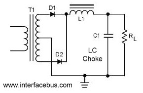
Full-Wave Rectifier circuit
A circuit that utilizes both positive and negative alternations in an alternating current to generate direct current. There are two types of full-wave rectifier circuits: one that employs two diodes and requires a center-tapped transformer, and another that uses four...