


ADUC832 1.3MIPS 8052 MCU + 62kB Flash + 8-Ch 12-Bit ADC + Dual 12-Bit DAC
#ADUC832
#8052 MCU
#12-bit ADC
#12-bit DAC
#data acquisition
#Flash microcontroller
#PQFP
#CSP
#MicroConverter
#ADI
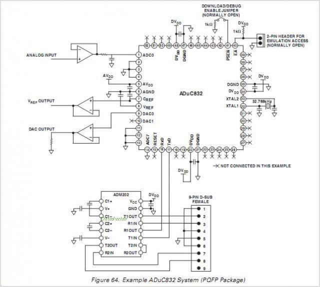
Description: The ADUC836 MicroConverter is a fully integrated 16-bit data acquisition system-on-a-chip. Like all of ADI's MicroConverter products, it features precision A/D and D/A conversion along with a Flash Microcontroller on a single chip. The ADUC836 is fully backward compatible (both hardware and software) with the ADuC816. It is available in 52-pin PQFP or 56-pin CSP packages and operates on a 3V or 5V power supply. The device functions with a 32 kHz crystal, utilizing an on-chip PLL to generate a high-frequency clock of 12.58 MHz. This clock is routed through a programmable clock divider, which produces the operating frequency for the MCU core clock. The Microcontroller core is based on the 8052 architecture, making it compatible with the 8051 instruction set, with 12 core clock periods per machine cycle.
The ADUC836 MicroConverter represents a significant advancement in integrated data acquisition systems, combining the functionality of analog-to-digital (A/D) and digital-to-analog (D/A) conversion along with a microcontroller in a single package. This integration facilitates compact design solutions for applications requiring precise data processing and control.
The device's compatibility with the ADuC816 ensures a smooth transition for users upgrading from previous models, minimizing the need for redesign efforts. The availability of both 52-pin PQFP and 56-pin CSP packages provides flexibility in design, allowing engineers to select the optimal footprint for their specific application needs.
Operating on a dual voltage of 3V or 5V enhances the versatility of the ADUC836, making it suitable for a wide range of applications, from battery-powered devices to more robust systems. The use of a 32 kHz crystal oscillator, paired with an on-chip phase-locked loop (PLL), enables the generation of a stable high-frequency clock at 12.58 MHz, which is essential for maintaining precise timing in data acquisition processes.
The programmable clock divider further enhances the device's flexibility, allowing designers to tailor the microcontroller core clock frequency to meet the requirements of their application. The 8052 core architecture ensures that existing 8051 code can be utilized without modification, thus streamlining development processes and reducing time-to-market.
In summary, the ADUC836 MicroConverter is a powerful and versatile solution for modern data acquisition needs, providing high precision, backward compatibility, and a range of operational features that cater to diverse electronic applications.The ADUC836 MicroConverter is a fully integrated 16-bit data acquisition system-on-a-chip. Like all of ADI`s MicroConverter products, it features precision A/D & D/A conversion and a Flash Microcontroller on a single chip. The ADUC836 is 100% backward compatible (hardware and software) with the ADuC816. It is available in 52-pin PQFP or 56-pin CSP packages and operates on a 3V or 5V power supply. The device operates from a 32 kHz crystal with an on-chip PLL generating a high frequency Clock of 12. 58 MHz. This Clock is routed through a programmable Clock divider from which the MCU core Clock operating frequency is generated.
The Microcontroller core is an 8052 and therefore 8051 instruction set compatible with 12 core Clock periods per machine cycle. By Analog Devices, Inc.
The ADUC836 MicroConverter represents a significant advancement in integrated data acquisition systems, combining the functionality of analog-to-digital (A/D) and digital-to-analog (D/A) conversion along with a microcontroller in a single package. This integration facilitates compact design solutions for applications requiring precise data processing and control.
The device's compatibility with the ADuC816 ensures a smooth transition for users upgrading from previous models, minimizing the need for redesign efforts. The availability of both 52-pin PQFP and 56-pin CSP packages provides flexibility in design, allowing engineers to select the optimal footprint for their specific application needs.
Operating on a dual voltage of 3V or 5V enhances the versatility of the ADUC836, making it suitable for a wide range of applications, from battery-powered devices to more robust systems. The use of a 32 kHz crystal oscillator, paired with an on-chip phase-locked loop (PLL), enables the generation of a stable high-frequency clock at 12.58 MHz, which is essential for maintaining precise timing in data acquisition processes.
The programmable clock divider further enhances the device's flexibility, allowing designers to tailor the microcontroller core clock frequency to meet the requirements of their application. The 8052 core architecture ensures that existing 8051 code can be utilized without modification, thus streamlining development processes and reducing time-to-market.
In summary, the ADUC836 MicroConverter is a powerful and versatile solution for modern data acquisition needs, providing high precision, backward compatibility, and a range of operational features that cater to diverse electronic applications.The ADUC836 MicroConverter is a fully integrated 16-bit data acquisition system-on-a-chip. Like all of ADI`s MicroConverter products, it features precision A/D & D/A conversion and a Flash Microcontroller on a single chip. The ADUC836 is 100% backward compatible (hardware and software) with the ADuC816. It is available in 52-pin PQFP or 56-pin CSP packages and operates on a 3V or 5V power supply. The device operates from a 32 kHz crystal with an on-chip PLL generating a high frequency Clock of 12. 58 MHz. This Clock is routed through a programmable Clock divider from which the MCU core Clock operating frequency is generated.
The Microcontroller core is an 8052 and therefore 8051 instruction set compatible with 12 core Clock periods per machine cycle. By Analog Devices, Inc.
Proximity Camera Head (A2047) Manual
The Proximity Camera Head (A2047) is a Long-Wire Data Acquisition (LWDAQ) device that interfaces with a TC255P image sensor. It is a radiation-tolerant evolution of the Inplane Sensor Head (A2036). The A2036 and A2033 are frequently used with the LWDAQ...
Data acquisition system
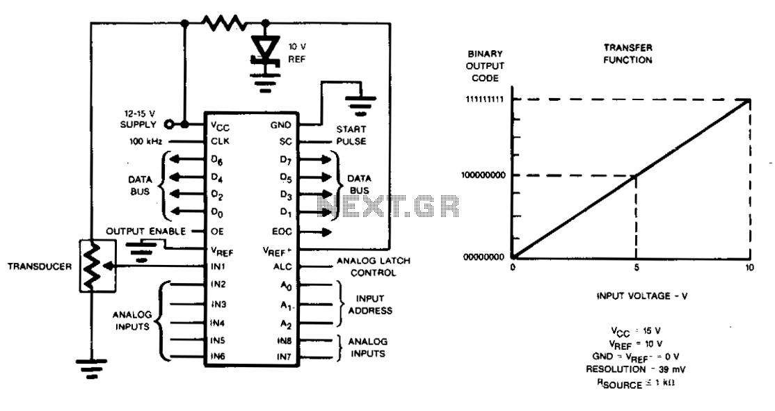
Charge redistribution is utilized to achieve analog-to-digital (A/D) conversion. In standard applications, this operates as a ratiometric conversion system for a microprocessor, where V^p is connected to ground and VREF+ is connected to Vcc. The output will provide a straightforward...
Based on one-chip computer data acquisition and wireless to receive and dispatch studying systematic
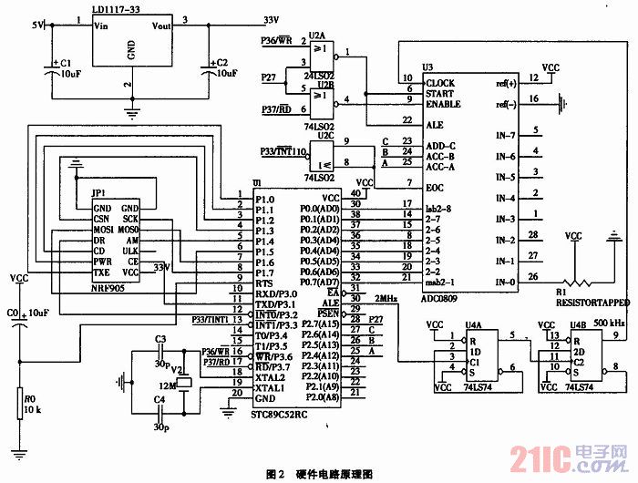
The technology of data acquisition is an important branch of information science. It is not only employed in intelligent instruments but is also widely used in modern industrial production and military science. This technology is essential for process control, condition...
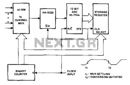
Data Acquisition System I
The HI-506 multiplexer functions as an analog input selector, which is controlled by a binary counter to select the appropriate channel. The HA-5330 serves as a high-speed sample and hold circuit. The sample/hold control is connected to the status (STS)...

acoustic daq mathematica
For physical computing or amateur science projects, it is often necessary to transfer the output from a sensor or transducer to a computer. Various methods exist for achieving this, utilizing specialized data acquisition hardware and software. This particular method is...
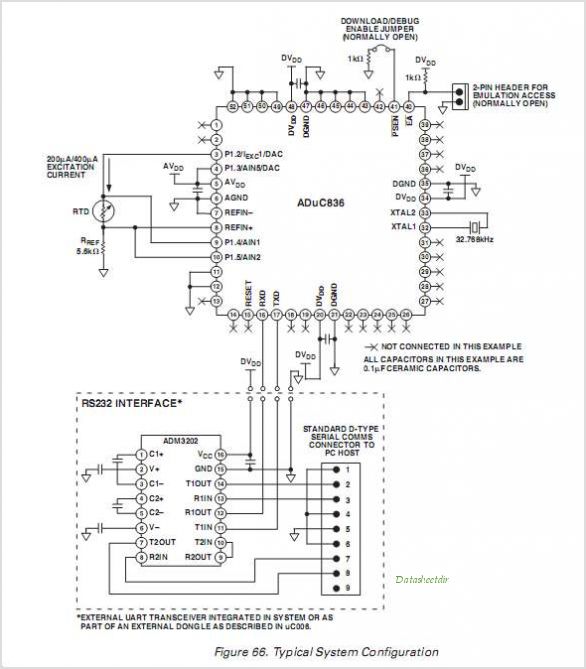
ADUC836 1MIPS 8052 MCU + 62kB Flash + Dual 16-Bit ADC + 12-Bit DAC
The ADUC841, ADUC842, and ADUC843 are complete smart transducer front ends that integrate a high-performance self-calibrating multichannel ADC, a dual DAC, and an optimized single-cycle 20 MHz 8-bit MCU (compatible with the 8051 instruction set) on a single chip. The...
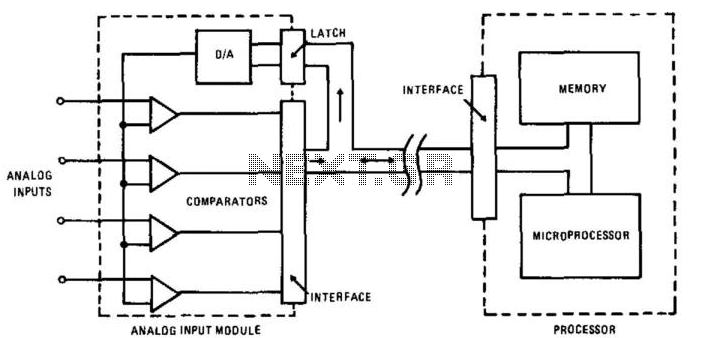
Data Acquisition System Ii
In this circuit, an HA-4900 series comparator is utilized alongside a digital-to-analog (D/A) converter to create a versatile, multichannel analog input for a data acquisition system. The processor first transmits an address to the D/A converter, after which it reads...
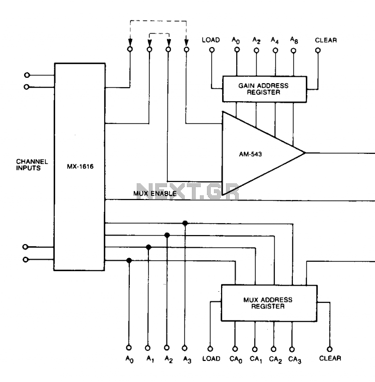
Fast data aquisition 1
This diagram illustrates a high-speed data acquisition system featuring eight differential inputs and a 12-bit resolution utilizing the AM-543. When the control logic is synchronized such that the Sample-Hold-ADC section converts one analog value while the mux-amplifier section stabilizes for...
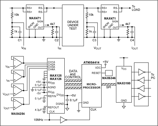
Practical Data Acquisition using a Windows based Power Meter
This application note outlines the design of a PC-based, 14-bit data acquisition system. It adopts a systematic approach, incorporating all essential components: analog, digital, hardware, and software. The document elaborates on each phase, emphasizing the testing of individual systems prior...