


gizDuino Hardware
#gizDuino
#ATmega
#program memory
#SRAM
#I/O pins
#Flash-based
#system clock
#CPU
#peripherals
#sketch
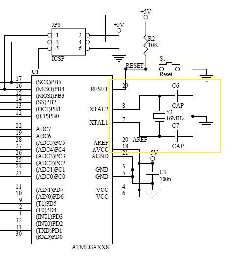
Description: The Flash-based program memory is where the program sketch is stored after an upload. The SRAM acts as the main memory where program variables are temporarily stored as the sketch executes. The system clock synchronizes the internal operation of the CPU and other peripherals. Of the ATmega's 23 programmable I/O pins, only 20 pins are available in the Arduino. Two pins are used by the oscillator circuit and one pin is used by the RESET, reducing the number of available I/O pins down to 20. The system clock circuitry of the ATmega generates a clean square wave signal that is used to synchronize the operations of the CPU and peripherals inside the microcontroller. The system clock performs a function that is analogous to what a traffic light does in managing traffic at an intersection. The ATmega normally requires an external oscillator circuit from which it derives the base clock. The oscillator circuit in the gizDuino board consists of a 16MHz crystal oscillator and two loading capacitors. It is connected to Pin 7 (XTAL1) and Pin 8 (XTAL2) of the ATmega. This is the same circuit found in the official Arduinos. Both ATmega328 and ATmega168 are rated to run at a full 20MHz clock speed; however, the Arduino team has opted for a 16MHz clock to maintain backward compatibility with older boards and avoid rewriting existing library routines. Additionally, both XTAL1 and XTAL2 pins also function as programmable I/O pins, with alternative names RB6 and RB7, respectively. They are part of the 23 I/Os of the ATmega328/168. For those planning to build a non-Arduino board using the ATmega328/168, there is an option to use these two pins as additional I/O by removing the external oscillator circuit and utilizing the internal 8MHz oscillator for the system clock.
The ATmega microcontroller serves as the heart of many Arduino-compatible boards, integrating essential functionalities through its architecture. The Flash-based memory is critical for storing the user-uploaded sketches, which are programs written in the Arduino programming language. The SRAM, or Static Random-Access Memory, plays a pivotal role in temporarily holding the variables and data utilized during program execution, ensuring efficient operation.
The system clock is a fundamental component, providing a timing reference for the CPU and peripheral devices. It generates a square wave signal that is instrumental in coordinating the microcontroller's operations, much like a traffic light orchestrates the flow of vehicles. The external oscillator circuit, typically consisting of a 16MHz crystal and associated capacitors, is essential for establishing the clock frequency. This circuit is connected to the designated pins on the ATmega, specifically XTAL1 and XTAL2, enabling the microcontroller to function at the desired clock rate.
The decision to use a 16MHz clock instead of the potential 20MHz capability of the ATmega328 and ATmega168 reflects a strategic choice by the Arduino development team. This choice prioritizes compatibility with legacy hardware and software, ensuring that existing projects and libraries remain functional without modification. However, it opens a discussion regarding the potential benefits of utilizing the full clock speed for performance improvements in future designs.
Moreover, the versatility of the ATmega's I/O pins is noteworthy. While certain pins are dedicated to specific functions, such as the oscillator and reset, others can be repurposed for general I/O tasks. This flexibility is particularly beneficial for custom board designs, allowing developers to maximize the utility of the microcontroller by leveraging the available pins effectively. The option to switch to the internal oscillator for applications that do not require high precision timing further enhances the adaptability of the ATmega328/168 in various projects.The Flash-based program memory is where the program sketch is stored after an upload. The SRAM act as the main memory where program variables are temporarily stored as the sketch executes. The system clock synchronizes the internal operation of the CPU and other peripherals. Of the ATmega`s 23 programmable I/O pins, only 20 pins are available in th e Arduino. Twopins are used by the oscillator circuit and 1 pin is used by the RESET, reducing the number of available I/O pins down to 20. The system clock circuitry of the ATmega generates a clean square wave signal that is used to synchronize the operations of the CPU and peripherals inside the microcontroller.
The system clock performs a function that is analogous to what a traffic light does in managing traffic in an intersection. The ATmega normally requires an external oscillator circuit where it derives the base clock. The oscillator circuit in the gizDuino board consists of a 16MHz crystal oscillator and two loading capacitors.
It is connected to Pin 7 (XTAL1) and Pin 8 (XTAL2) of the ATmega, as shown below. As to be expected, this is the same circuit found in the official Arduinos. Now, a little rant: with both ATmega328 and ATmega168 rated to run at a full 20Mhz clock speed, I can not help but wonder why the Arduino team settled for a much slower 16Mhz clock. Granted that they probably choose backward-compatibility with their older boards and eliminate rewrite of the existing library routines, I still think it has to be done sooner than later.
With several Arduino boards already existing, a version that runs on a full 20-Mhz speed would, at least, be nice addition. End of little rant. As already note previously, both XTAL1 and XTAL2 pins also function as programmable I/O pins. Both pins have alternative names of RB6 and RB7, respectively; they are part of the 23 I/Os of the ATmega328/168.
Just in case you are planning to build a non-Arduino board that uses the ATmega328/168, you can have the option of using these two pins as additional I/O. Simply remove the external oscillator circuit and, instead, use the internal 8MHz oscillator for the system clock.
The ATmega microcontroller serves as the heart of many Arduino-compatible boards, integrating essential functionalities through its architecture. The Flash-based memory is critical for storing the user-uploaded sketches, which are programs written in the Arduino programming language. The SRAM, or Static Random-Access Memory, plays a pivotal role in temporarily holding the variables and data utilized during program execution, ensuring efficient operation.
The system clock is a fundamental component, providing a timing reference for the CPU and peripheral devices. It generates a square wave signal that is instrumental in coordinating the microcontroller's operations, much like a traffic light orchestrates the flow of vehicles. The external oscillator circuit, typically consisting of a 16MHz crystal and associated capacitors, is essential for establishing the clock frequency. This circuit is connected to the designated pins on the ATmega, specifically XTAL1 and XTAL2, enabling the microcontroller to function at the desired clock rate.
The decision to use a 16MHz clock instead of the potential 20MHz capability of the ATmega328 and ATmega168 reflects a strategic choice by the Arduino development team. This choice prioritizes compatibility with legacy hardware and software, ensuring that existing projects and libraries remain functional without modification. However, it opens a discussion regarding the potential benefits of utilizing the full clock speed for performance improvements in future designs.
Moreover, the versatility of the ATmega's I/O pins is noteworthy. While certain pins are dedicated to specific functions, such as the oscillator and reset, others can be repurposed for general I/O tasks. This flexibility is particularly beneficial for custom board designs, allowing developers to maximize the utility of the microcontroller by leveraging the available pins effectively. The option to switch to the internal oscillator for applications that do not require high precision timing further enhances the adaptability of the ATmega328/168 in various projects.The Flash-based program memory is where the program sketch is stored after an upload. The SRAM act as the main memory where program variables are temporarily stored as the sketch executes. The system clock synchronizes the internal operation of the CPU and other peripherals. Of the ATmega`s 23 programmable I/O pins, only 20 pins are available in th e Arduino. Twopins are used by the oscillator circuit and 1 pin is used by the RESET, reducing the number of available I/O pins down to 20. The system clock circuitry of the ATmega generates a clean square wave signal that is used to synchronize the operations of the CPU and peripherals inside the microcontroller.
The system clock performs a function that is analogous to what a traffic light does in managing traffic in an intersection. The ATmega normally requires an external oscillator circuit where it derives the base clock. The oscillator circuit in the gizDuino board consists of a 16MHz crystal oscillator and two loading capacitors.
It is connected to Pin 7 (XTAL1) and Pin 8 (XTAL2) of the ATmega, as shown below. As to be expected, this is the same circuit found in the official Arduinos. Now, a little rant: with both ATmega328 and ATmega168 rated to run at a full 20Mhz clock speed, I can not help but wonder why the Arduino team settled for a much slower 16Mhz clock. Granted that they probably choose backward-compatibility with their older boards and eliminate rewrite of the existing library routines, I still think it has to be done sooner than later.
With several Arduino boards already existing, a version that runs on a full 20-Mhz speed would, at least, be nice addition. End of little rant. As already note previously, both XTAL1 and XTAL2 pins also function as programmable I/O pins. Both pins have alternative names of RB6 and RB7, respectively; they are part of the 23 I/Os of the ATmega328/168.
Just in case you are planning to build a non-Arduino board that uses the ATmega328/168, you can have the option of using these two pins as additional I/O. Simply remove the external oscillator circuit and, instead, use the internal 8MHz oscillator for the system clock.
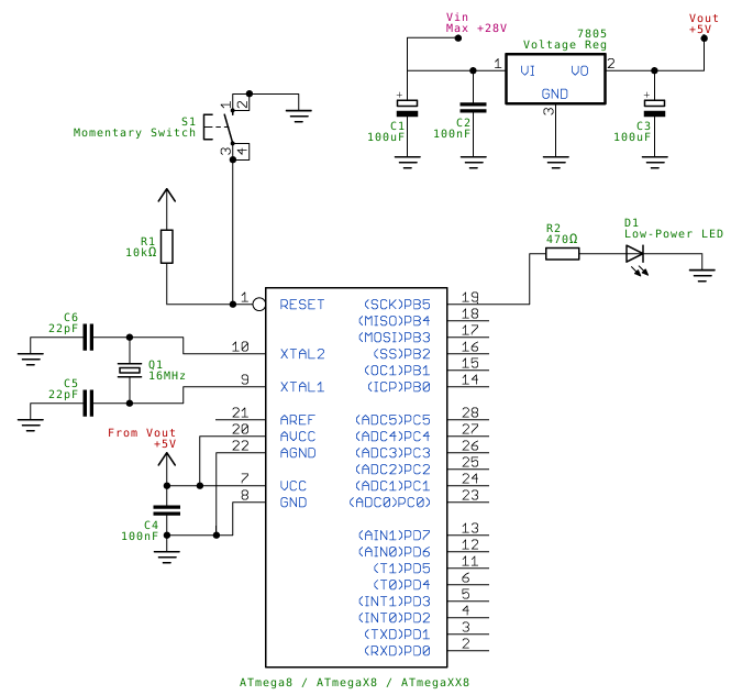
atmega
After compiling a C or C++ program into an AVR binary using AVR-GCC, the next step is to "burn" the binary onto the chip. This can be accomplished with one of three applications: AVRDUDE, UISP, or AVR Studio. To enable...
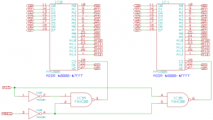
Mark 2 Memory circuit
The memory component of the Mark 2 system is quite straightforward. It consists of two 32K SRAM chips, which are actually FRAM due to availability, but this does not impact functionality in this context. The selection of these chips is...
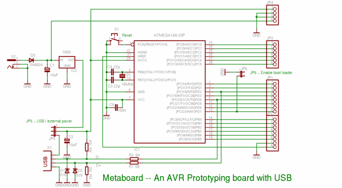
ems metaboard
Any microcontroller from the ATmegaXX8 family can be utilized, although investing a small amount in additional flash memory is advisable. A DIP socket is technically optional, but its absence is not recommended. A 28-pin DIP socket is somewhat uncommon; if...
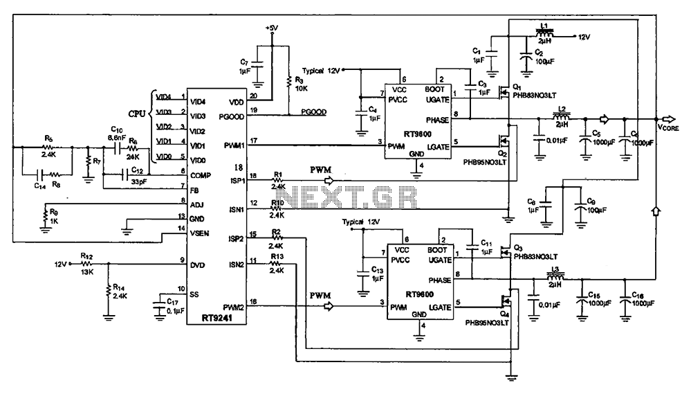
A typical computer motherboard CPU power supply circuit
A typical computer motherboard CPU power supply circuit is primarily composed of the main power supply management chip RT9241 and additional components from the power management chip RT9600. The voltage command signal from the CPU is input into the RT9241,...
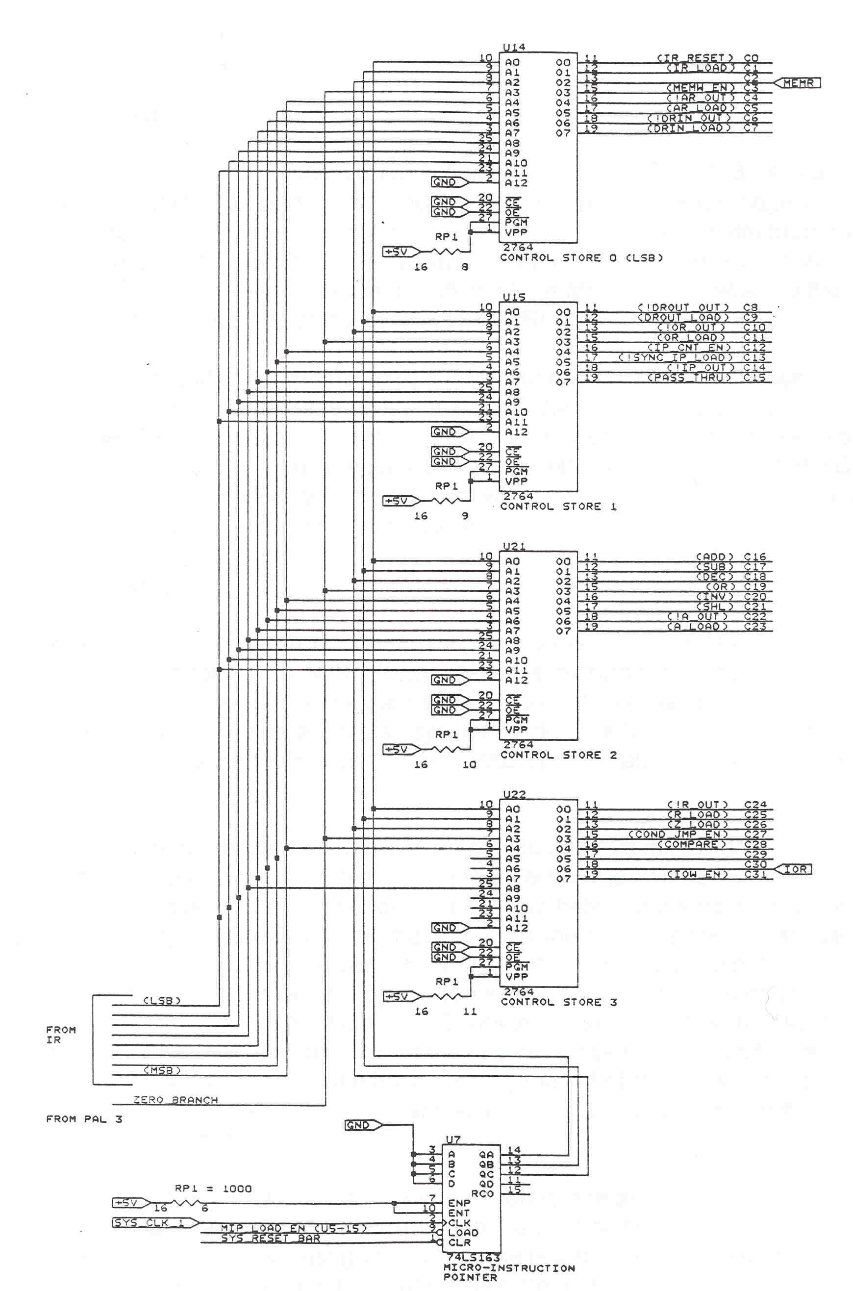
P8 CPU Documentatio Hardware
The datapath consists of registers, an ALU, and an internal system bus. Registers are fast memory locations internal to the CPU, distinct from main system memory, and serve as temporary storage during calculations. The ALU is a combinational logic device...