


Wiring up to the AN2131
#AN2131
#GPIO
#crystal oscillator
#power regulators
#key matrix
#protoboard
#floating pins
#input/output
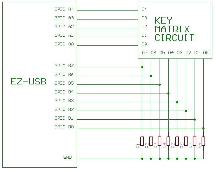
Description: The circuit utilizes an AN2131 chip accompanied by the necessary support components, including a crystal oscillator and power regulators. The inputs and outputs of the key matrix were connected to the GPIO ports of the AN2131 through a protoboard. However, this setup encountered issues where the keys would frequently become "stuck." This problem arose from unconnected chip pins that could "float" between on and off states due to residual charge in the wiring. To resolve this, pull-down resistors were incorporated to allow any residual charge to discharge to ground when the keys are released. One pull-down resistor was added to each input of the circuit, utilizing various spare resistors ranging from 320 ohms to 1000 ohms.
The AN2131 chip is a microcontroller designed for handling input and output operations, particularly in embedded systems. The integration of a crystal oscillator is critical for providing a stable clock signal, ensuring the microcontroller operates at the desired frequency. Power regulators are essential for supplying the appropriate voltage levels to the AN2131 and supporting components, maintaining operational integrity.
The key matrix serves as an interface for user input, where each key press corresponds to a unique signal. The GPIO ports of the AN2131 are configured to read these signals. However, without proper termination, floating inputs can lead to erratic behavior, such as keys appearing to be continuously pressed. The implementation of pull-down resistors effectively mitigates this issue by ensuring that the GPIO pins are pulled to a low state when not actively driven high by a key press.
The choice of pull-down resistor values, ranging from 320 ohms to 1000 ohms, indicates a consideration for both power consumption and response time. Lower resistance values will provide a quicker discharge of residual charge but may draw slightly more current when the keys are pressed. Conversely, higher resistance values reduce current draw but may result in slower response times. The final circuit diagram would illustrate the connections between the AN2131, the key matrix, and the pull-down resistors, ensuring clarity in the design and functionality of the circuit.It`s just a AN2131 chip with the required support circuitry - crystal oscillator, power regulators etc. First I took the inputs and outputs of the key matrix and wired them to the GPIO ports of the AN2131.
This was just a matter of plugging the whole lot into some protoboard. This didn`t work too well, as the keys would get "stuck" often. This is because an unconnected chip leg can "float" between on and off due to the residual charge held in the wire. The solution is to add pull-down resistors which allow this residual charge to flow to ground when the key is released. I added one to each input of the circuit. I used a variety of spare resistors from the junk box 320 ohms to 1000 ohms. This is the final circuit diagram:
The AN2131 chip is a microcontroller designed for handling input and output operations, particularly in embedded systems. The integration of a crystal oscillator is critical for providing a stable clock signal, ensuring the microcontroller operates at the desired frequency. Power regulators are essential for supplying the appropriate voltage levels to the AN2131 and supporting components, maintaining operational integrity.
The key matrix serves as an interface for user input, where each key press corresponds to a unique signal. The GPIO ports of the AN2131 are configured to read these signals. However, without proper termination, floating inputs can lead to erratic behavior, such as keys appearing to be continuously pressed. The implementation of pull-down resistors effectively mitigates this issue by ensuring that the GPIO pins are pulled to a low state when not actively driven high by a key press.
The choice of pull-down resistor values, ranging from 320 ohms to 1000 ohms, indicates a consideration for both power consumption and response time. Lower resistance values will provide a quicker discharge of residual charge but may draw slightly more current when the keys are pressed. Conversely, higher resistance values reduce current draw but may result in slower response times. The final circuit diagram would illustrate the connections between the AN2131, the key matrix, and the pull-down resistors, ensuring clarity in the design and functionality of the circuit.It`s just a AN2131 chip with the required support circuitry - crystal oscillator, power regulators etc. First I took the inputs and outputs of the key matrix and wired them to the GPIO ports of the AN2131.
This was just a matter of plugging the whole lot into some protoboard. This didn`t work too well, as the keys would get "stuck" often. This is because an unconnected chip leg can "float" between on and off due to the residual charge held in the wire. The solution is to add pull-down resistors which allow this residual charge to flow to ground when the key is released. I added one to each input of the circuit. I used a variety of spare resistors from the junk box 320 ohms to 1000 ohms. This is the final circuit diagram:
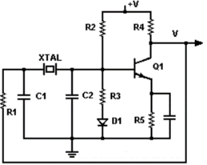
crystal oscillator discreet pierce oscillator
There are various configurations for crystal oscillators, with the most common being discrete and integrated circuits like the Pierce and RLC Bridge. The discrete Pierce oscillator is a suitable choice when good frequency stability and a relatively simple circuit are...
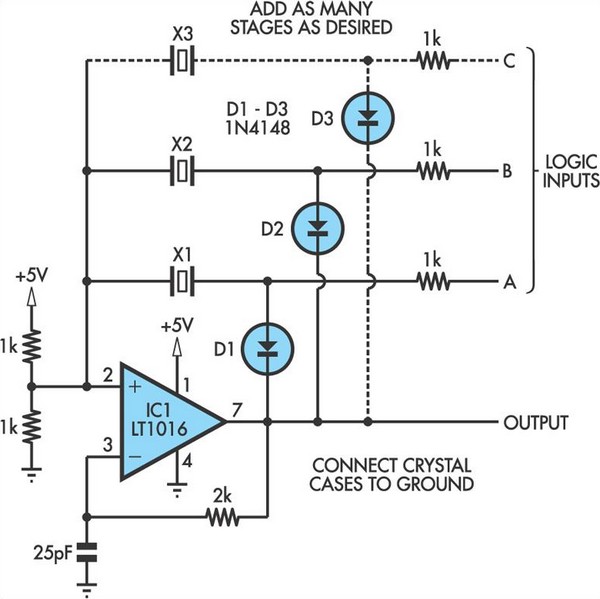
Switchable Output Crystal Oscillator
This oscillator circuit allows crystals to be electronically switched by logic commands. To understand the circuit, it is helpful to initially disregard all crystals and consider all diodes as shorts while their associated 1kΩ resistors are treated as open. The...
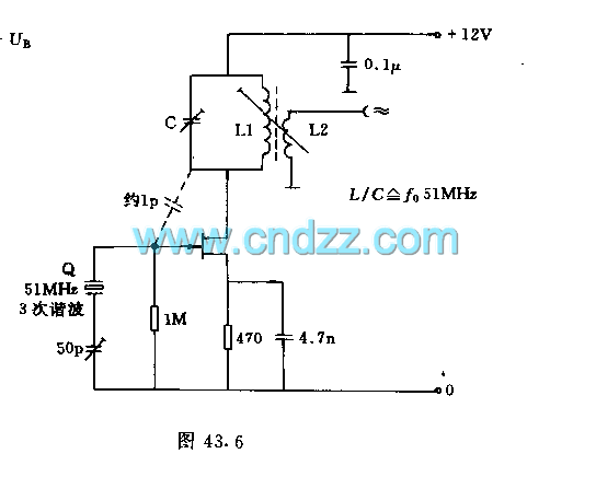
Crystal quartz crystal oscillator circuit using FET
A crystal oscillator operates at a frequency of 51 MHz, which corresponds to the third harmonic of a 17 MHz fundamental frequency. Depending on the specific structure used, the drain-gate capacitance can be selected within a range of 0.5 to...
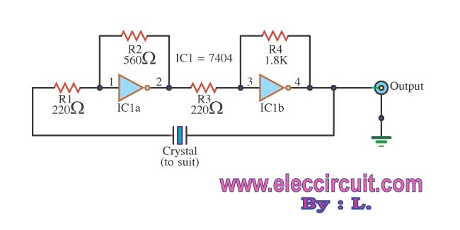
Crystal oscillator using TTL
The circuit operates using binary signal statuses of "1" and "0". It also incorporates a frequency generator.
The circuit described utilizes a binary signaling system, which is fundamental in digital electronics. The binary states "1" and "0" represent the two possible...
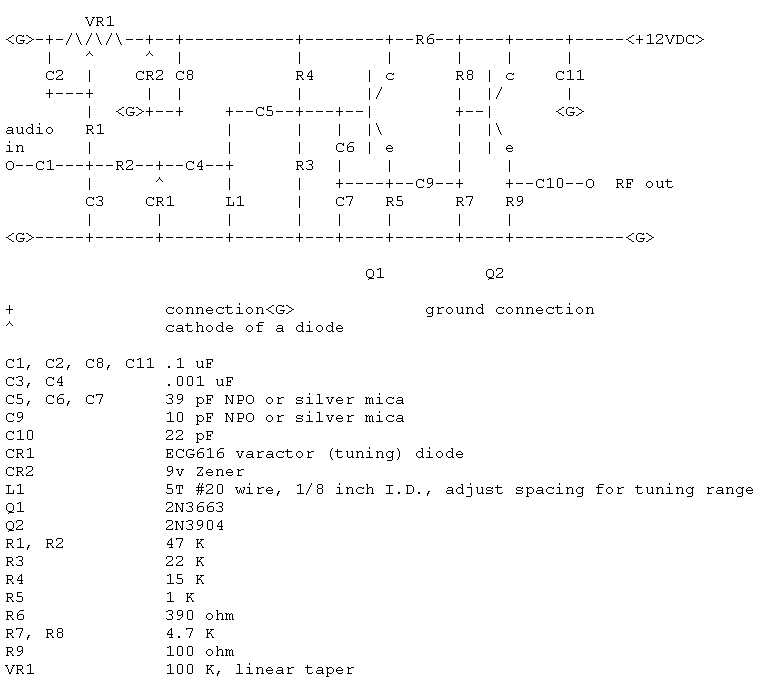
Crystal Oscillator II
The world is full of xtal oscillators twiddled by digital designers lacking in the analog design knowledge necessary. Just look at all the PC real time clocks that lags or leads by several minutes per day. And they eat backup...
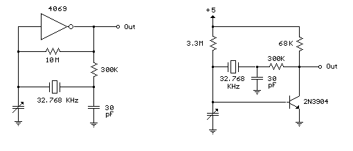
Oscillator using crystal
Below are a couple circuits you can use to produce a 32.768 KHz square wave from a common watch crystal. The output can be fed to a 15 stage binary counter to obtain a 1 second square wave. The circuit...

Third-overtone crystal oscillator
This circuit utilizes a 74S00 Schottky TTL gate. Additionally, no inductors are necessary.
The 74S00 is a dual 4-input NAND gate that operates at high speeds due to its Schottky technology, which minimizes propagation delay and power consumption. The circuit design...
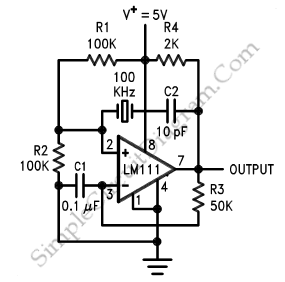
Crystal Oscillator
A crystal oscillator, particularly a low-frequency variant, can be effectively constructed using an operational amplifier (op-amp) as the amplification component. Below is the schematic diagram of this circuit.
The crystal oscillator circuit utilizes the properties of a quartz crystal to generate...
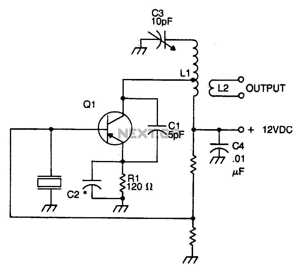
Overtone crystal oscillator
The crystal element in this circuit is connected directly between the base and ground. Capacitor C1 is utilized to enhance feedback due to the internal capacitances of the transistor. This capacitor should be positioned as close as possible to the...