


1khz multiple feedback low pass filter circuit
#low pass filter
#op-amp
#multiple feedback
#1kHz
#filter circuit
#signal processing
#active filter
#trim pins
#floating pins
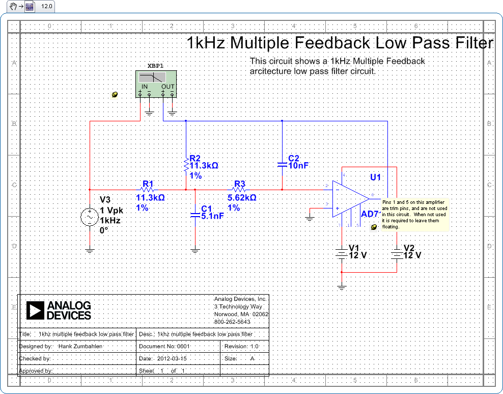
Description: Pins 1 and 5 on this amplifier are trim pins and are not utilized in the circuit. When not in use, it is necessary to leave them floating.
In electronic amplifier circuits, trim pins are often included for calibration or adjustment purposes, but they may not always be necessary for the amplifier's operation. In this case, pins 1 and 5 are designated as trim pins, indicating that they serve no function in the current configuration of the circuit. It is essential to ensure that these pins remain unconnected or "floating" to prevent any unintended effects on the amplifier's performance.
Floating these pins means that they should not be connected to ground or any voltage source, as this can introduce noise or instability in the amplifier's operation. Proper handling of unused pins is crucial in maintaining the integrity of the circuit and ensuring optimal performance.
When designing or implementing this amplifier circuit, attention must be paid to the layout and connections to avoid accidentally connecting these trim pins to other circuit elements. Careful documentation and adherence to the schematic will facilitate correct assembly and operation of the amplifier, ensuring that it functions as intended without interference from unused components.Pins 1 and 5 on this amplifier are trim pins and are not used in the circuit. When not used it is required to leave them floating.
In electronic amplifier circuits, trim pins are often included for calibration or adjustment purposes, but they may not always be necessary for the amplifier's operation. In this case, pins 1 and 5 are designated as trim pins, indicating that they serve no function in the current configuration of the circuit. It is essential to ensure that these pins remain unconnected or "floating" to prevent any unintended effects on the amplifier's performance.
Floating these pins means that they should not be connected to ground or any voltage source, as this can introduce noise or instability in the amplifier's operation. Proper handling of unused pins is crucial in maintaining the integrity of the circuit and ensuring optimal performance.
When designing or implementing this amplifier circuit, attention must be paid to the layout and connections to avoid accidentally connecting these trim pins to other circuit elements. Careful documentation and adherence to the schematic will facilitate correct assembly and operation of the amplifier, ensuring that it functions as intended without interference from unused components.Pins 1 and 5 on this amplifier are trim pins and are not used in the circuit. When not used it is required to leave them floating.
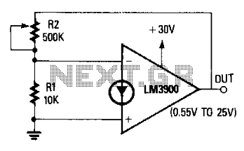
Variable-Voltage Reference Source
The non-inverting terminal of the operational amplifier (op-amp) is grounded, and the circuit utilizes the voltage at the inverting terminal as a reference. The voltage gain of the circuit is determined by the ratio of resistors R2 to R. When...
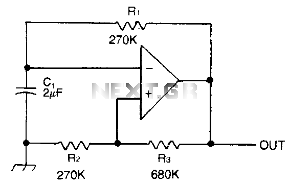
Single-op-amp-clock
Capacitor C1 is charged through timing resistor R1 when the clock output is high. When C1 reaches the upper threshold voltage, the output signal decreases, and then C1 discharges through R1 until its voltage reaches the lower threshold point. When...
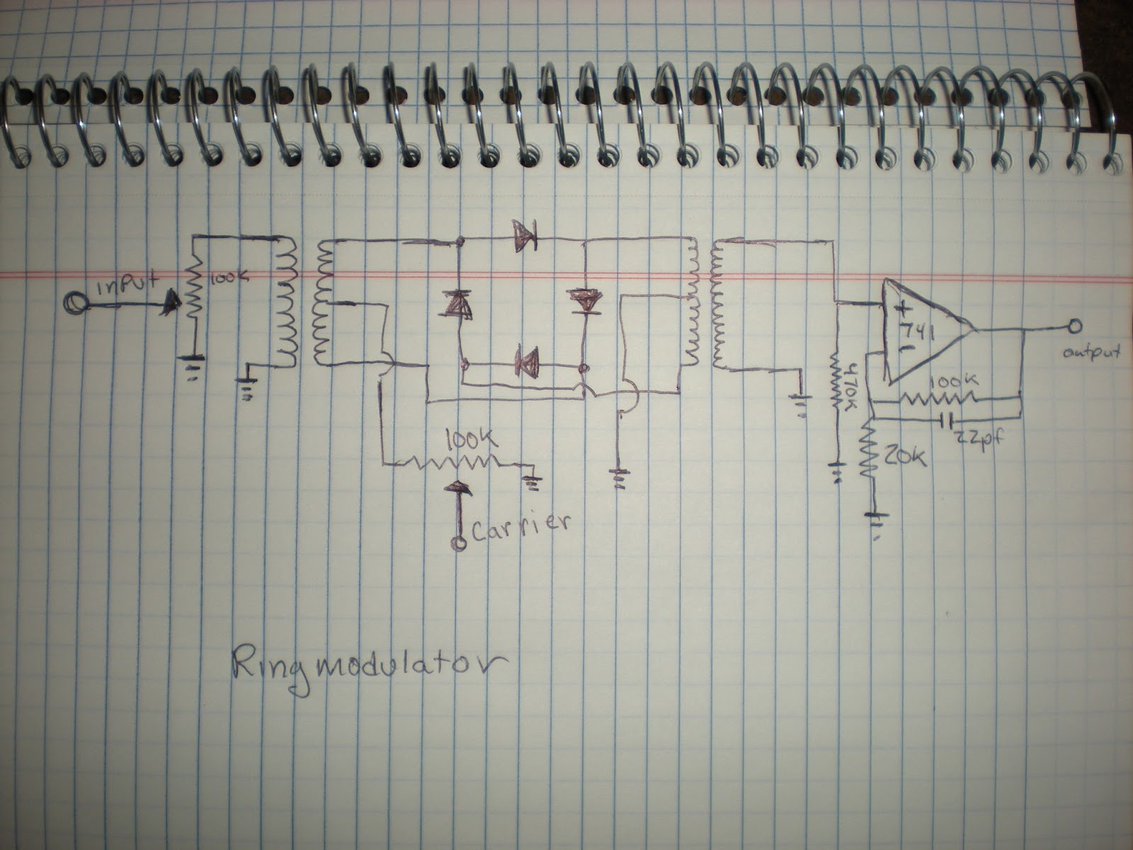
Ring Modulator
The author has created various modules since the last blog post and has gained a deeper understanding of electronics, particularly with operational amplifiers (Op Amps). The author does not guarantee the designs shared, as they are an amateur learning through...
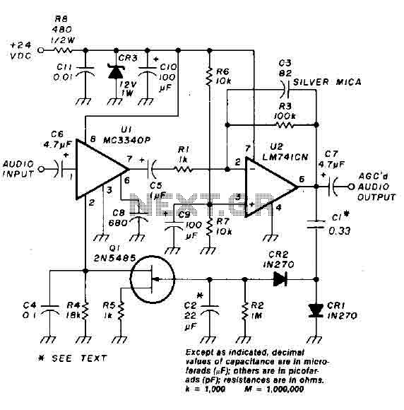
Auto gain control op-amp circuit
An audio signal applied to the input VI is passed through the operational amplifier 741, designated as U2. After amplification, the output signal V2 is sampled and sent to a negative voltage doubler/rectifier circuit composed of diodes CR1 and CR2,...
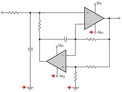
Single Supply Active Filter with Virtual Ground
All filter stages utilizing a Virtual Ground will exhibit the Virtual Ground DC potential at their outputs, whereas all stages employing a resistive divider at their input (without a Virtual Ground) will present the divider potential at their output. For...
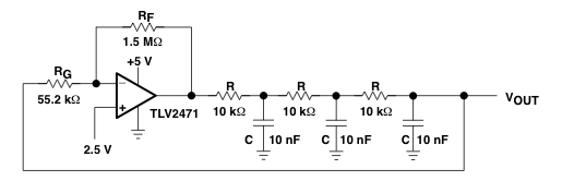
a better sine wave
The operational amplifier (op-amp) is configured for 50x amplification, functioning similarly to a comparator. With this setup, a 50 mV deviation from the 2.5V reference will push the output to its limits. The output signal resembles a heavily clipped sine...
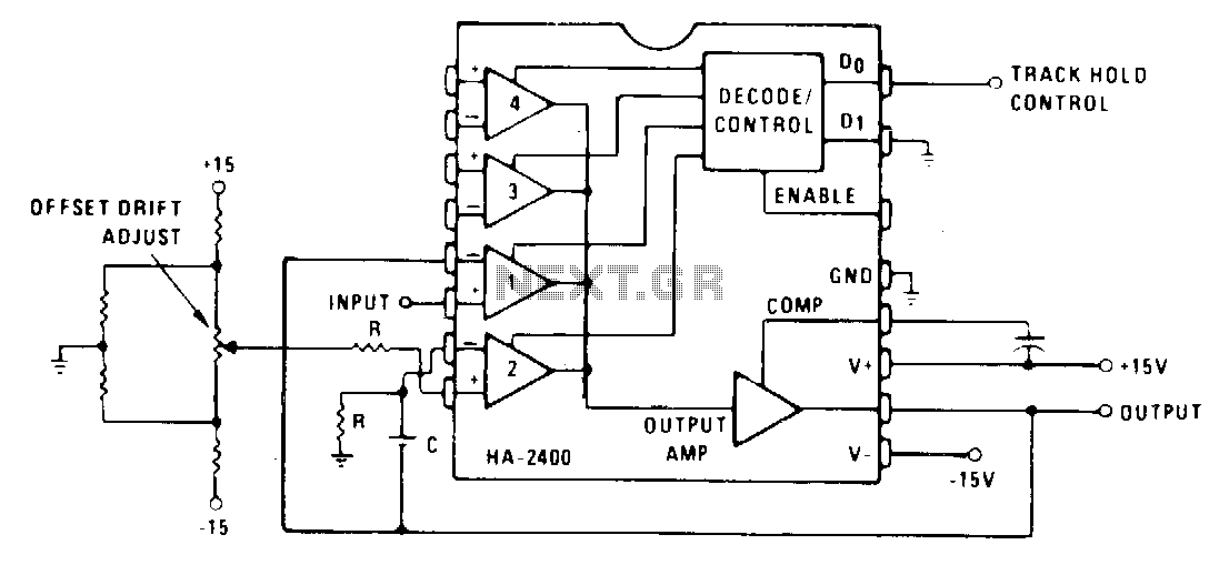
Track-and-hold-sample-and-hold
Channel 1 is configured as a voltage follower and is activated during the track/sample time. If the product of R and C is sufficiently short compared to the period of maximum output frequency or sample time, then C will charge...
op amp ringer circuit old telephone
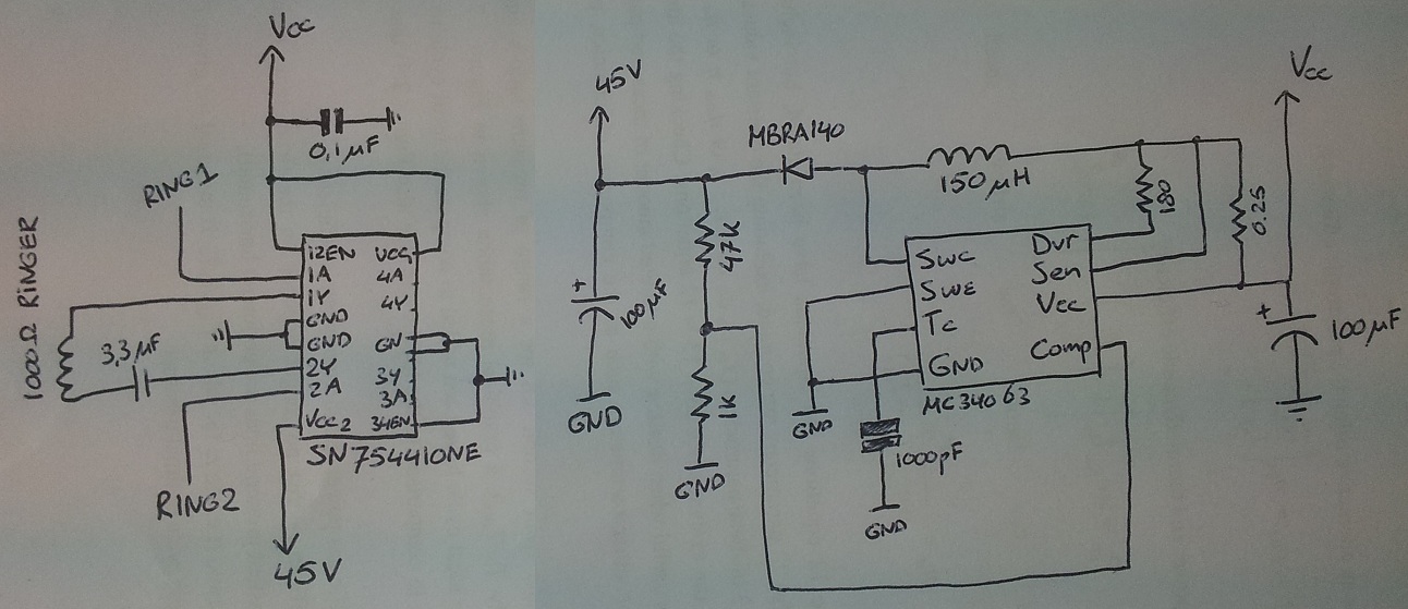
The process involves adapting an old phone for Bluetooth functionality, specifically testing the ringer circuit constructed using schematics from Sparkfun. When connecting a section of the schematic to a 3.5V source (Vcc), an output voltage of 45V is observed, with...
Capacitive load driver
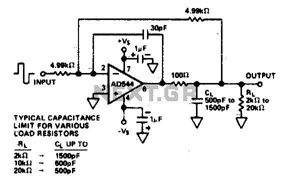
The circuit utilizes a 100-ohm isolation resistor that allows the amplifier to drive capacitive loads greater than 500 pF. This resistor effectively isolates high-frequency feedback from the load, contributing to circuit stability. Low-frequency feedback is returned to the amplifier's summing...