


A feedback circuit and the differential input stage bias circuit is provided separately
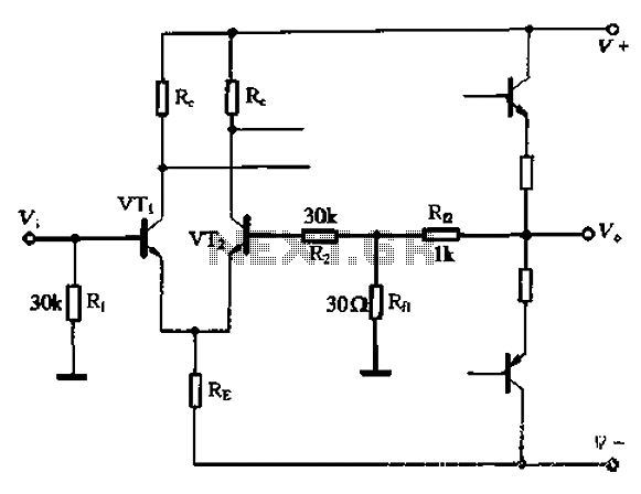
Description: The circuit utilizes the configuration illustrated in Figure 1-36, with the feedback circuit and bias circuit implemented separately. The feedback resistor, Rfl, is approximately 30 ohms. To maintain the desired amplification, the resistor R queue is set to 1 kilo-ohm between the base and the right transistor's emitter, while the resistor Rtz matches the left transistor's base resistance. The value of resistor R2 is such that R2 is equal to R1, ensuring that the bias remains consistent on both sides without reducing the input resistance.
The circuit configuration described is typical in amplifier designs where feedback and biasing are critical for maintaining performance and stability. The feedback resistor, Rfl, plays a significant role in determining the overall gain of the amplifier. By setting Rfl to approximately 30 ohms, the circuit can achieve a specific level of feedback that stabilizes the gain and reduces distortion.
The resistor R queue, placed between the base and the right transistor's emitter, is crucial for controlling the input impedance and ensuring that the transistor operates within its optimal range. The choice of 1 kilo-ohm for R queue is a standard practice to balance the input characteristics of the amplifier.
In addition, the matching of the left and right transistor base resistances via Rtz ensures that both transistors operate symmetrically, which is essential for minimizing discrepancies in amplification and maintaining linearity across the circuit. The careful selection of R2 to equal R1 further reinforces this symmetry, allowing for consistent biasing across both sides of the circuit. This design consideration helps to prevent input resistance reduction, which could adversely affect the circuit's performance.
Overall, the described circuit demonstrates a thoughtful approach to amplifier design, focusing on feedback, biasing, and input resistance to achieve reliable and efficient operation. Circuit using the form shown in Figure 1-36, the feedback circuit and the bias circuit separately, Rfl take about 30fl. To ensure put magnification, R queue take lkflo between the base and the right pipe string Rtz same people and left tube base resistance R value resistor R2, so that R2 Rl F30kfIO such bias can be consistent on both sides, and input resistance is not reduced.
The circuit configuration described is typical in amplifier designs where feedback and biasing are critical for maintaining performance and stability. The feedback resistor, Rfl, plays a significant role in determining the overall gain of the amplifier. By setting Rfl to approximately 30 ohms, the circuit can achieve a specific level of feedback that stabilizes the gain and reduces distortion.
The resistor R queue, placed between the base and the right transistor's emitter, is crucial for controlling the input impedance and ensuring that the transistor operates within its optimal range. The choice of 1 kilo-ohm for R queue is a standard practice to balance the input characteristics of the amplifier.
In addition, the matching of the left and right transistor base resistances via Rtz ensures that both transistors operate symmetrically, which is essential for minimizing discrepancies in amplification and maintaining linearity across the circuit. The careful selection of R2 to equal R1 further reinforces this symmetry, allowing for consistent biasing across both sides of the circuit. This design consideration helps to prevent input resistance reduction, which could adversely affect the circuit's performance.
Overall, the described circuit demonstrates a thoughtful approach to amplifier design, focusing on feedback, biasing, and input resistance to achieve reliable and efficient operation. Circuit using the form shown in Figure 1-36, the feedback circuit and the bias circuit separately, Rfl take about 30fl. To ensure put magnification, R queue take lkflo between the base and the right pipe string Rtz same people and left tube base resistance R value resistor R2, so that R2 Rl F30kfIO such bias can be consistent on both sides, and input resistance is not reduced.
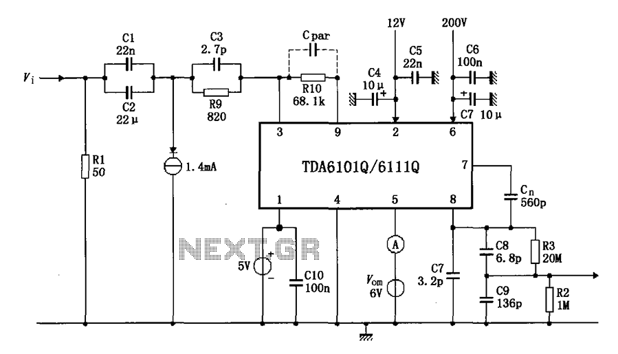
Test circuit diagram with feedback factor of 1 83 DA6101Q 6111Q
The test circuit features a feedback factor of 1/83 utilizing the DA6101Q/6111Q. The input signal is fed through a network comprising resistors R1 and R9, and capacitors C1, C2, and C3, entering the TDA6101Q, which includes three pins for the...
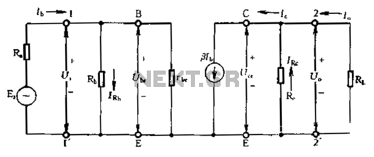
Calculate magnification input resistance and output resistance circuit
Calculate magnification, input resistance, and output resistance circuit.
This circuit is designed to calculate the magnification, input resistance, and output resistance of a given electronic system. The magnification refers to the ratio of the output signal to the input signal, which...
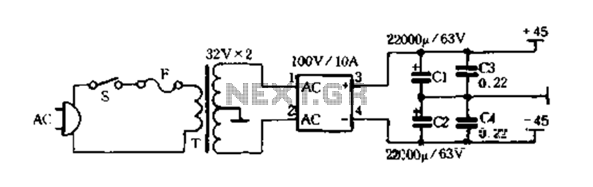
Simple quality-oriented PA 02
The differential input stage utilizes the integrated differential transistors 2SC1583 and 2SA798, with the amplified signal directed to the power amplifier tubes VT5 and VT6. The performance of the charge directly influences the overall performance of the power amplifier circuit....
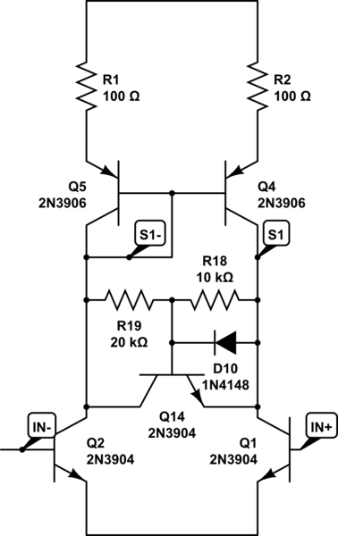
amplifier How to improve nasty form clipping behavior in differential input stage
The amplifier in the following schematic, when simulated, demonstrates the ability to effectively amplify a signal with an amplitude of 0.1V to 10V. However, when subjected to a larger input signal, the performance deteriorates significantly during the positive half cycle,...
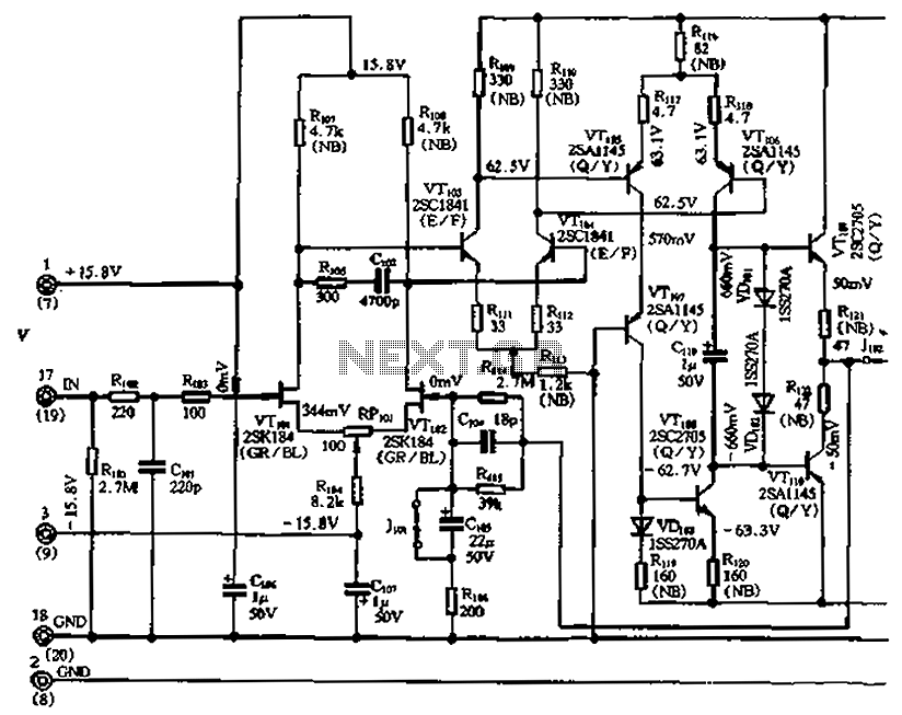
No linear feedback amplifier circuit a
The circuit features a differential input stage that implements differential voltage amplification, forced differential voltage amplification, and a complementary push-pull amplifier output. It includes a bias circuit, a distortion servo circuit, and a protection circuit. The input preamplifier stage is...