


ADA4858-3 used as a PIN diode driver circuit
#ADA4858-3
#PIN diode
#buffer gate
#TTL
#signal swing
#driver circuit
#operational amplifier
#voltage swing
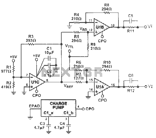
Description: The circuit can incorporate a buffer gate at the input to ensure compatibility with TTL or other logic levels. This design is intended for a TTL 0V circuit to accommodate a 3.5V input signal swing. Additionally, it generates a complementary -1.5V to +3.5V swing for driving PIN diodes. Resistors R1, R2, and R3, along with operational amplifier U1C, create a -1.5V reference voltage for the circuit, utilizing the internal negative voltage produced by the charge pump. Capacitors C3 and C4 are essential for the operation of the charge pump.
The described circuit functions as a voltage level translator and signal conditioner, facilitating the integration of different logic families. The buffer gate at the input serves to isolate the input signal from subsequent stages, thereby preventing loading effects that could distort the signal integrity. The compatibility with TTL logic levels allows for seamless interfacing with various digital circuits.
The generation of a -1.5V reference voltage is crucial for applications that require bipolar signal swings, such as driving PIN diodes, which are commonly used in RF and photonic applications. The resistors R1, R2, and R3 are configured to establish this reference voltage by forming a voltage divider network. This network ensures that the output of the operational amplifier U1C accurately reflects the desired reference level while maintaining stability against variations in supply voltage.
The internal charge pump plays a pivotal role in generating the necessary negative voltage. By utilizing capacitors C3 and C4, the charge pump can effectively store and transfer charge, enabling the creation of the -1.5V output. The selection of these capacitors is critical; their values must be chosen to balance the charge transfer efficiency and the response time of the charge pump circuit.
In summary, this circuit design not only provides a robust solution for interfacing different logic levels but also ensures the proper operation of components like PIN diodes through the generation of a stable negative voltage reference. The careful selection of components and their configurations is essential to achieve optimal performance in various electronic applications.The figure can add a buffer gate at the input, so that the circuit compatible with TTL or other logic. This request is to TTL0V circuit to 3.5V input signal swing to a complementary -1.5V to + 3.5V swing for driving PIN diodes. R1, R2, R3 and U1C formed -1.5V reference voltage of the circuit, the internal negative voltage CPO produced by the internal charge pump. The charge pump capacitors C3 and C4 are necessary for the work.
The described circuit functions as a voltage level translator and signal conditioner, facilitating the integration of different logic families. The buffer gate at the input serves to isolate the input signal from subsequent stages, thereby preventing loading effects that could distort the signal integrity. The compatibility with TTL logic levels allows for seamless interfacing with various digital circuits.
The generation of a -1.5V reference voltage is crucial for applications that require bipolar signal swings, such as driving PIN diodes, which are commonly used in RF and photonic applications. The resistors R1, R2, and R3 are configured to establish this reference voltage by forming a voltage divider network. This network ensures that the output of the operational amplifier U1C accurately reflects the desired reference level while maintaining stability against variations in supply voltage.
The internal charge pump plays a pivotal role in generating the necessary negative voltage. By utilizing capacitors C3 and C4, the charge pump can effectively store and transfer charge, enabling the creation of the -1.5V output. The selection of these capacitors is critical; their values must be chosen to balance the charge transfer efficiency and the response time of the charge pump circuit.
In summary, this circuit design not only provides a robust solution for interfacing different logic levels but also ensures the proper operation of components like PIN diodes through the generation of a stable negative voltage reference. The careful selection of components and their configurations is essential to achieve optimal performance in various electronic applications.The figure can add a buffer gate at the input, so that the circuit compatible with TTL or other logic. This request is to TTL0V circuit to 3.5V input signal swing to a complementary -1.5V to + 3.5V swing for driving PIN diodes. R1, R2, R3 and U1C formed -1.5V reference voltage of the circuit, the internal negative voltage CPO produced by the internal charge pump. The charge pump capacitors C3 and C4 are necessary for the work.
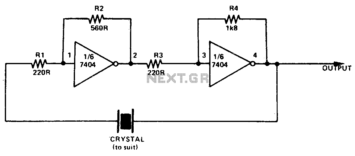
Simple ttl crystal oscillator
This simple and inexpensive crystal oscillator consists of one-third of a 7404 IC, four resistors, and a crystal. The inverters are biased into their linear regions by resistors R1 to R4, while the crystal provides the necessary feedback. Oscillation can...
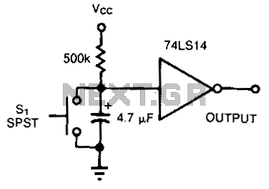
Switch-debouncer
The TTL inverter 74LS14 features an internal 16-kohm pull-up resistor that ensures the gate input is pulled high when the switch is open. Upon closing the switch, a 4.7uF capacitor discharges at the initial contact. If the switch contacts bounce...
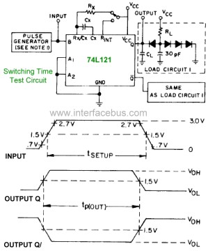
74121 IC Description TTL Monostable Multivibrator IC
The pinout diagram for the 74L121 and 74L122 integrated circuits (ICs) is applicable to any style of 74xx121 or 74xx122 dual in-line package (DIP) chip, although the timing graphs are only relevant for the indicated TTL families. The 74121 provides...
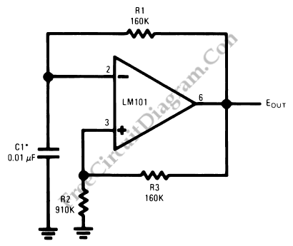
Operational Amplifier (Op-Amp) Oscillator
This is an operational amplifier (Op-Amp) oscillator circuit. This circuit has several advantages, including its ability to operate at low frequencies.
The operational amplifier oscillator circuit is designed to generate a periodic waveform output, typically a sine or square wave, using...
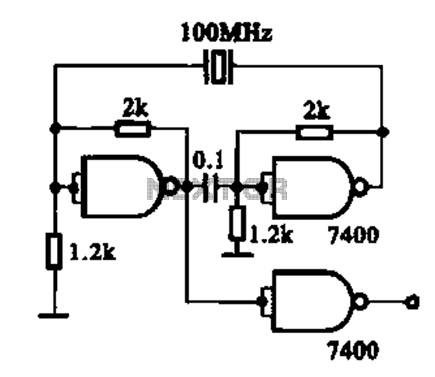
TTL integrated circuits made of a crystal oscillator
Crystal oscillator integrated circuits, specifically two diagrams of oscillator circuits with oscillation frequencies of 10 MHz and 20 MHz.
Crystal oscillators are essential components in various electronic applications, providing stable frequency references for timing and synchronization purposes. The circuits presented include...
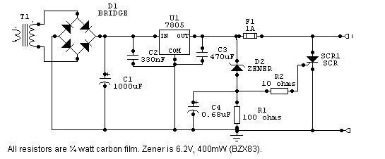
Power Supply for TTL
In the circuit shown below, if the voltage at the output terminals rises above 6.2V, zener conducts charging capacitor C4. This voltage will fire the silicon-controlled rectifier (SCR), which quickly shorts across the supply rails blowing the fuse. The regulator...
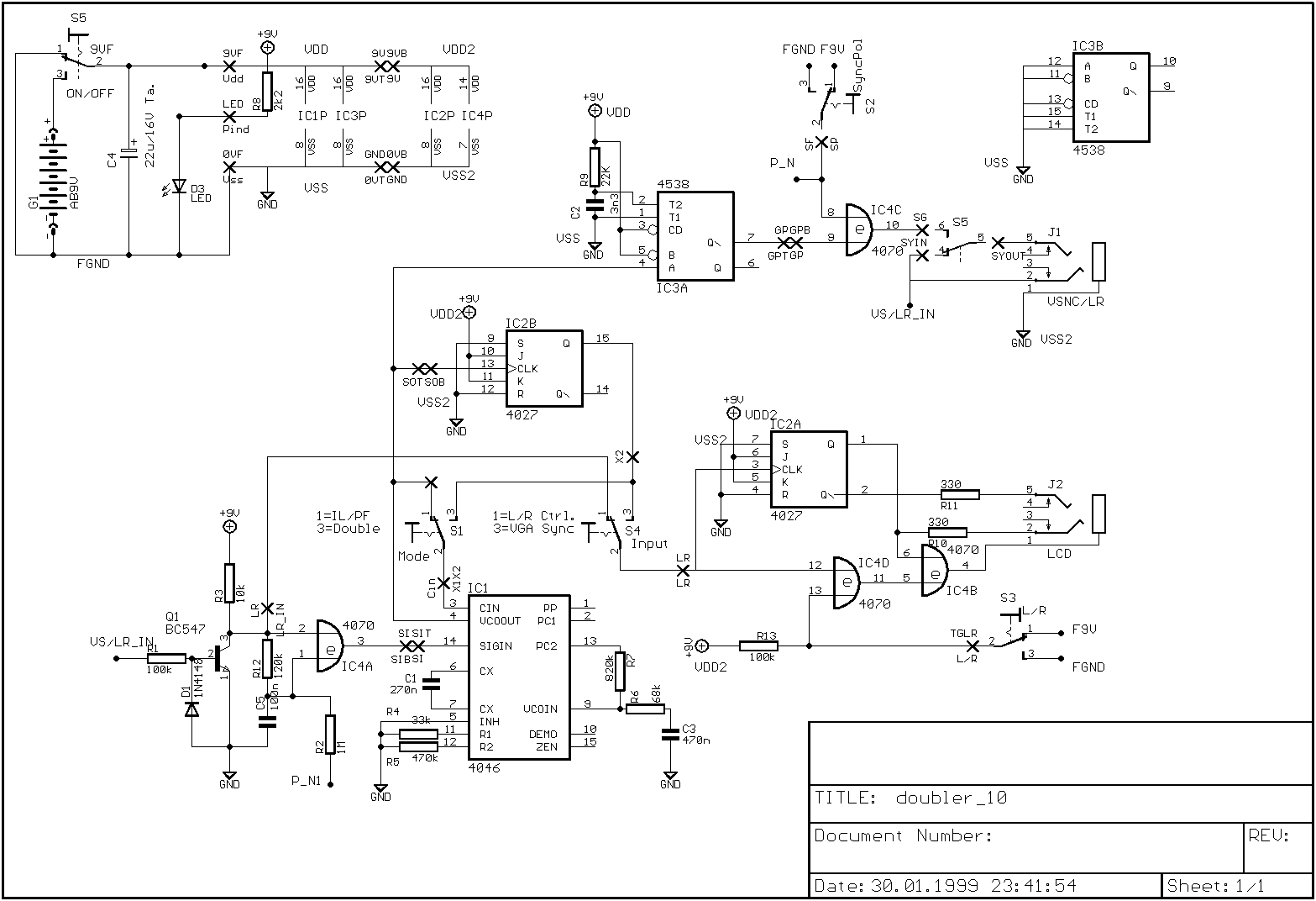
LCD_controller
The clip sync output to TTL level appears to require additional time to accommodate extra components on the board. As a temporary solution, a ZPD4.7 (4.7 V Zener Diode) should be placed between SG and ground at the power switch...
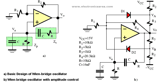
Opamp Wien-bridge oscillator
The Wien-bridge oscillator consists of an operational amplifier (OA) in a non-inverting configuration with a gain of 1 + R2/R1 and an RC feedback network.
The Wien-bridge oscillator is a type of electronic oscillator that generates sine waves. It employs a...
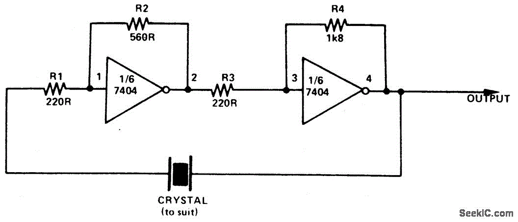
SIMPLE TTL CRYSTAL OSCILLATOR
This simple and inexpensive crystal oscillator consists of one-third of a 7404 hex inverter, four resistors, and a crystal. The inverters are biased into their linear regions by resistors R1 to R4, while the crystal provides the necessary feedback. Oscillation...