


BALANCED MODULATOR
#modulator
#differential amplifiers
#carrier signal
#switching function
#RF
#signal processing
#communication
#electronics
#circuit design
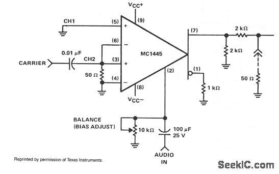
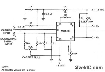
Description: When the carrier level is sufficient to activate the cross-coupled pair of differential amplifiers, the modulation signal applied to the gate will switch at the carrier frequency between the collector loads. This switching process results in the modulation being multiplied by a symmetrical switching function. If the gate remains within the linear region, only the first harmonic will be present. To achieve balance in the MC1445 modulator, equal gain must be attained in the two separate channels. To maintain operation in the linear region, the modulation input should be limited to approximately 200 mV peak-to-peak. Due to the sensitivity of the gate bias point to carrier suppression, a high-resolution, 10-turn potentiometer is recommended.
In this electronic circuit, the MC1445 modulator is employed to facilitate the modulation of signals using a carrier frequency. The cross-coupled differential amplifiers play a crucial role in this modulation process, enabling the switching of the modulation signal at the carrier rate. This is essential for applications requiring precise signal modulation, such as in communication systems.
The modulation signal's switching is influenced by the carrier level, which must be adequately set to ensure effective operation of the differential amplifiers. The symmetrical switching function generated during the modulation process is important for maintaining signal integrity. If the gate operates within the linear region, it ensures that only the first harmonic component is present, which is critical for reducing unwanted distortions in the output signal.
To balance the performance of the MC1445 modulator, it is vital to achieve equal gain across both channels. This balancing act is essential for maintaining signal fidelity and ensuring that the modulation characteristics remain consistent. The limitation of the modulation input to approximately 200 mV peak-to-peak is a design consideration that helps keep the system operating within the linear region, thus preventing distortion.
The sensitivity of the gate bias point to carrier suppression highlights the necessity for precise adjustments in the circuit. The use of a high-resolution, 10-turn potentiometer allows for fine-tuning of the bias point, ensuring optimal performance and stability of the modulation process. This attention to detail in component selection and circuit design is crucial for achieving reliable operation in various electronic applications.When the carrier level is adequate to switch the cross-coupled pair of differential amplifiers, the modulation signal, which has been applied to the gate, will be switched at the carrier rate, between the collector loads. When switching occurs, it will result in the modulation being multiplied by a symmetrical switching function.
If the modulation gate remains in the linear region, only the first harmonic will be present. To balance the MC1445 modulator, equal gain must be achieved in the two separate channels. To remain in the linear region, the modulation input must be restricted to approximately 200 mV pk-pk. Because the gate bias point is sensitive to the amount of carrier suppression, a high-resolution, 10-turn potentiometer should be used.
In this electronic circuit, the MC1445 modulator is employed to facilitate the modulation of signals using a carrier frequency. The cross-coupled differential amplifiers play a crucial role in this modulation process, enabling the switching of the modulation signal at the carrier rate. This is essential for applications requiring precise signal modulation, such as in communication systems.
The modulation signal's switching is influenced by the carrier level, which must be adequately set to ensure effective operation of the differential amplifiers. The symmetrical switching function generated during the modulation process is important for maintaining signal integrity. If the gate operates within the linear region, it ensures that only the first harmonic component is present, which is critical for reducing unwanted distortions in the output signal.
To balance the performance of the MC1445 modulator, it is vital to achieve equal gain across both channels. This balancing act is essential for maintaining signal fidelity and ensuring that the modulation characteristics remain consistent. The limitation of the modulation input to approximately 200 mV peak-to-peak is a design consideration that helps keep the system operating within the linear region, thus preventing distortion.
The sensitivity of the gate bias point to carrier suppression highlights the necessity for precise adjustments in the circuit. The use of a high-resolution, 10-turn potentiometer allows for fine-tuning of the bias point, ensuring optimal performance and stability of the modulation process. This attention to detail in component selection and circuit design is crucial for achieving reliable operation in various electronic applications.When the carrier level is adequate to switch the cross-coupled pair of differential amplifiers, the modulation signal, which has been applied to the gate, will be switched at the carrier rate, between the collector loads. When switching occurs, it will result in the modulation being multiplied by a symmetrical switching function.
If the modulation gate remains in the linear region, only the first harmonic will be present. To balance the MC1445 modulator, equal gain must be achieved in the two separate channels. To remain in the linear region, the modulation input must be restricted to approximately 200 mV pk-pk. Because the gate bias point is sensitive to the amount of carrier suppression, a high-resolution, 10-turn potentiometer should be used.
Amatorki projekt
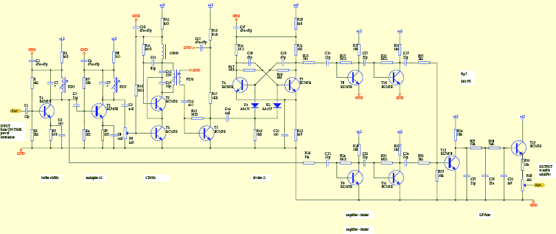
The circuit is designed to add two identical branches to the existing despreading spectrum. The only difference between the branches is the phase of the PN sequences fed into each branch, specifically at the input of a double-balanced mixer. The...
Reflex Radio Receiver
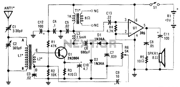
The RF signal is transmitted from the antenna through CI to a tuned circuit consisting of LI and C2. One end of L2 delivers the RF signal to the base of Q1 for amplification, while the other end connects to...
Radio harmonic detection circuit
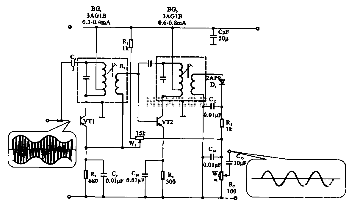
The demodulation and detection circuit is a radio AM intermediate frequency (IF) signal amplifier that performs two-stage detection using diode Dr. It extracts the audio signal from the IF carrier detection and subsequently sends it to the power amplifier stage....
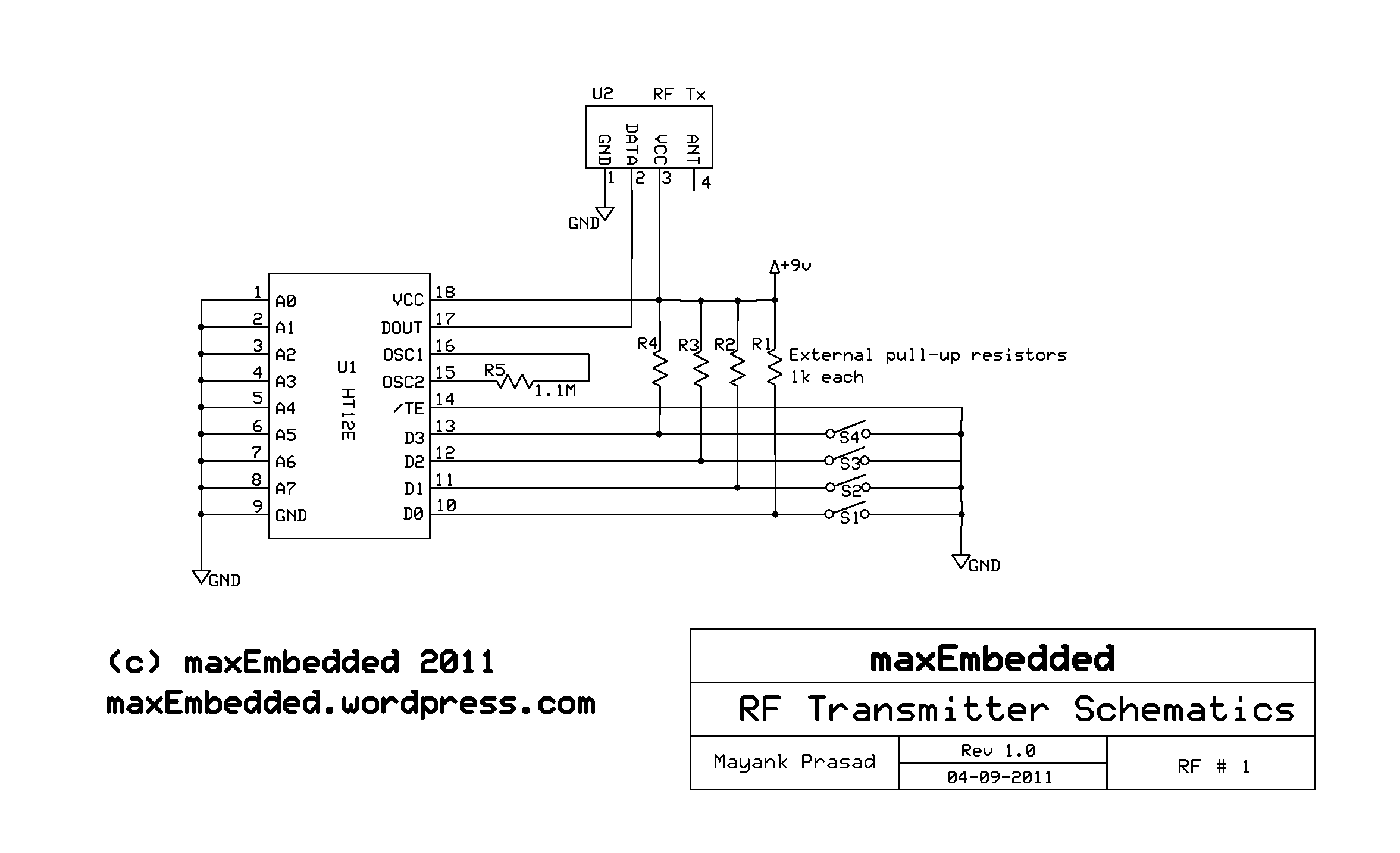
making an rf car
This article is authored by Yash Tambi, a Core Committee Member of roboVITics. It discusses RF-controlled robots, which are among the simplest types of robots. The essential components include a few readily available integrated circuits (ICs), a 433 MHz transmitter...
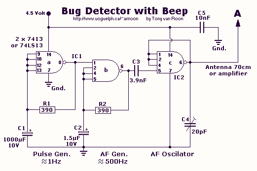
RF Bug detector
This circuit is not open for discussion. Although working perfectly, it was experimental. I will answer no emails in regards to this circuit. If you are looking for a more serious and reliable bug detector, go to the Countersurveillance Monitor...
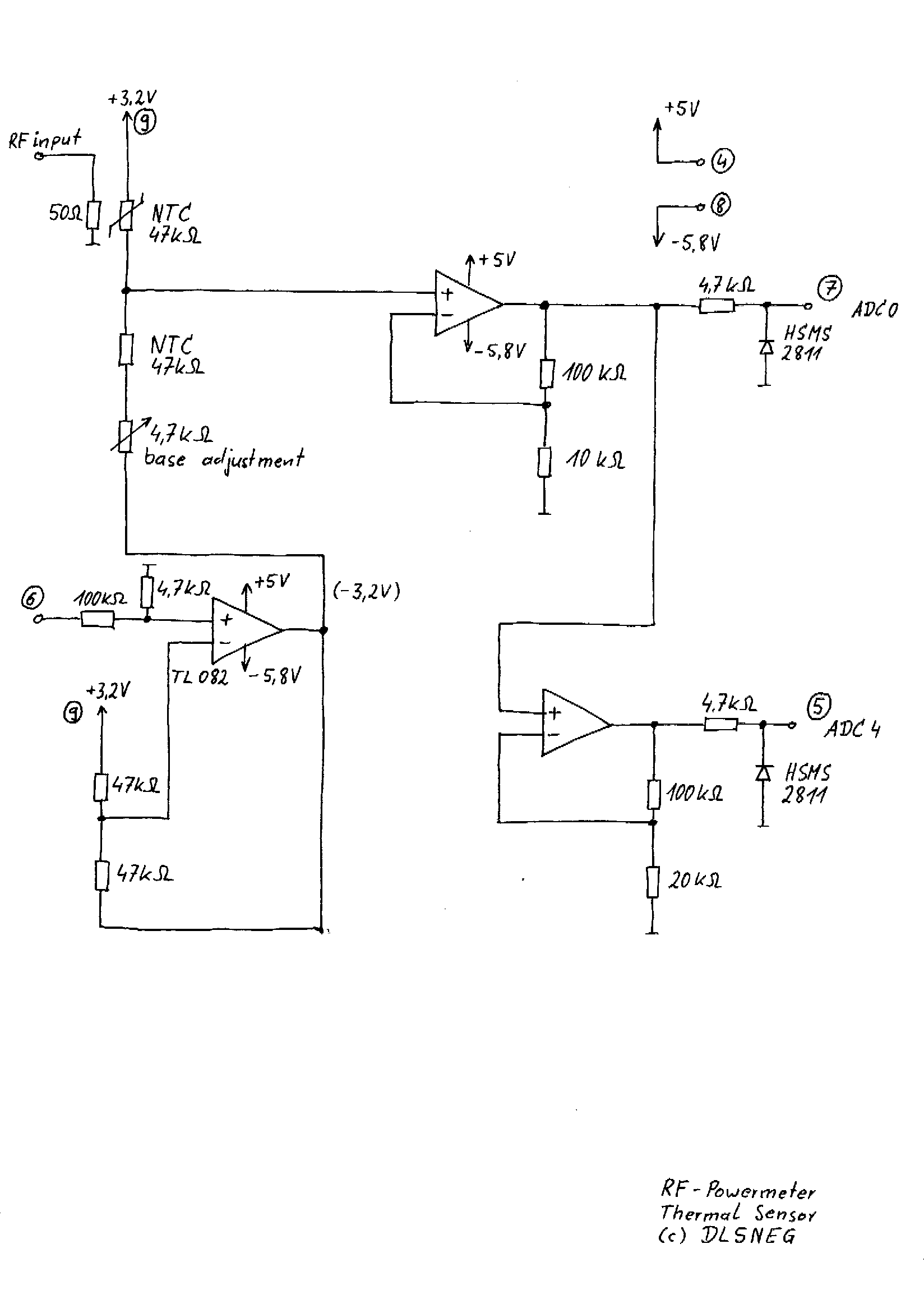
handheld RF-Powermeter for multiple sensors up to 12 GHz
A few years ago, a diode-sensor based RF power meter was built using a 68HC11 microprocessor. Prior to that, an analog RF power meter with a thermal power sensor was developed. The datasheets for logarithmic amplifiers, which promised a measurement...
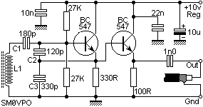
Basic RF Oscillator
Create a basic RF oscillator. The circuit is very simple, so complex calculations will be omitted, and component selection will be simplified using calculators. For this example, the target frequency is 7 MHz. The circuit includes a transistor (TR1) on...

Transmitter RF Output LED Indicator
Transmitter RF Output LED Indicator Circuit Diagram. This RF output detector circuit, which includes a visual indicator, can be useful for an RF application.
The transmitter RF output LED indicator circuit is designed to provide a visual representation of the RF...
DOUBLE SIDEBAND SUPPRESSED CARRIER MODULATOR
The basic current allows no carrier to be present in the output. By adding offsets to the carrier differential pairs, controlled amounts of carrier appear at the output. The amplitude becomes a function of the modulation signal—AM modulation.
In a typical...