


Converting current to voltage transducer circuit Using LM107
#LM107
#current to voltage
#transducer
#amplifier
#measurement
#signal conversion
#precision
#analog circuits
#impedance
#error reduction
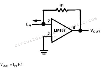
Description: Converting current into voltage is undesirable for two reasons: first, an impedance is inserted into the measuring line, causing an error; second, amplifier offset voltage is also amplified, leading to a subsequent loss of accuracy. The use of a current-to-voltage transducer avoids both of these problems. This circuit functions as a current-to-voltage transducer. The input current is fed directly into the summing node, and the amplifier output voltage changes to extract the same current from the summing node through resistor R1. The scale factor of this circuit is R1 volts per amp. The only conversion error in this circuit is Ibias, which is summed algebraically with IIN.
The described circuit operates as a current-to-voltage transducer, effectively converting input current into a proportional output voltage while minimizing measurement errors. The input current (IIN) is directly applied to a summing node, which is a key feature of this configuration. This node is typically part of an operational amplifier (op-amp) setup, where the characteristics of the op-amp play a crucial role in the overall performance of the transducer.
In this circuit, resistor R1 is employed to set the scale factor, establishing a direct relationship between the input current and the output voltage. The output voltage (VOUT) can be expressed mathematically as VOUT = IIN * R1, indicating that for every ampere of input current, the output voltage increases by R1 volts. This linearity is essential for accurate signal processing in various applications, including sensor interfacing and data acquisition systems.
The presence of Ibias, the input bias current of the operational amplifier, introduces a minor error in the output voltage. This bias current is summed with the input current, which can lead to deviations from the ideal output. However, in well-designed circuits, this error can often be minimized through careful selection of components and circuit layout, ensuring that the impact of Ibias is negligible in the overall performance.
Overall, this current-to-voltage transducer circuit is a reliable solution for applications requiring precise current measurements, providing a linear output voltage that can be easily interfaced with analog-to-digital converters or other signal processing components. The design considerations surrounding the choice of resistor values, op-amp specifications, and layout techniques are critical for achieving optimal performance and accuracy in practical implementations.Converting into voltage is undesirable for two reasons: first, an impedance is inserted into the measuring line causing an error; second, amplifier offset voltage is also amplified with a subsequent loss of accuracy. The use of a current to voltage transducer avoids both of these problems. This is current to voltage transducer circuit. The input c urrent is fed directly into the summing node and the amplifier output voltage changes to extract the same current from the summing node through R1. The scale factor of this circuit is R1 volts per amp. The only conversion error in this circuit is Ibias which is summed algebraically with IIN. Here is a schematic drawing :
The described circuit operates as a current-to-voltage transducer, effectively converting input current into a proportional output voltage while minimizing measurement errors. The input current (IIN) is directly applied to a summing node, which is a key feature of this configuration. This node is typically part of an operational amplifier (op-amp) setup, where the characteristics of the op-amp play a crucial role in the overall performance of the transducer.
In this circuit, resistor R1 is employed to set the scale factor, establishing a direct relationship between the input current and the output voltage. The output voltage (VOUT) can be expressed mathematically as VOUT = IIN * R1, indicating that for every ampere of input current, the output voltage increases by R1 volts. This linearity is essential for accurate signal processing in various applications, including sensor interfacing and data acquisition systems.
The presence of Ibias, the input bias current of the operational amplifier, introduces a minor error in the output voltage. This bias current is summed with the input current, which can lead to deviations from the ideal output. However, in well-designed circuits, this error can often be minimized through careful selection of components and circuit layout, ensuring that the impact of Ibias is negligible in the overall performance.
Overall, this current-to-voltage transducer circuit is a reliable solution for applications requiring precise current measurements, providing a linear output voltage that can be easily interfaced with analog-to-digital converters or other signal processing components. The design considerations surrounding the choice of resistor values, op-amp specifications, and layout techniques are critical for achieving optimal performance and accuracy in practical implementations.Converting into voltage is undesirable for two reasons: first, an impedance is inserted into the measuring line causing an error; second, amplifier offset voltage is also amplified with a subsequent loss of accuracy. The use of a current to voltage transducer avoids both of these problems. This is current to voltage transducer circuit. The input c urrent is fed directly into the summing node and the amplifier output voltage changes to extract the same current from the summing node through R1. The scale factor of this circuit is R1 volts per amp. The only conversion error in this circuit is Ibias which is summed algebraically with IIN. Here is a schematic drawing :
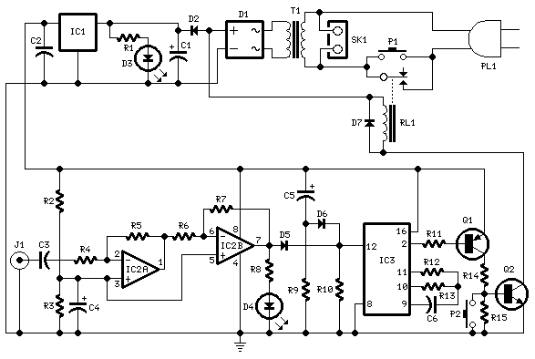
Amplifier Timer
This circuit deactivates an amplifier or other devices when a low-level audio signal at its input is absent for at least 15 minutes. By pressing P1, the device is activated, supplying power to any appliance connected to SK1. The input...

Amplifier Cool-Down Circuit Circuit
This cool-down relay circuit utilizes an integrated circuit (IC) timer to control a relay, which maintains the operation of the blower for a specified time delay determined by timer U3. The capacitance value of C2 can be adjusted to either...
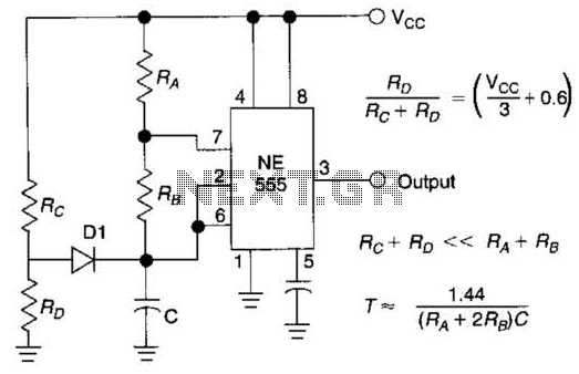
Precision Lf Oscillator Circuit
Using Rl, R7, and D1 to preset CI to one third of the supply voltage. This circuit avoids a longer first cycle period than subsequent cycles.
The circuit described involves the use of resistors Rl and R7 along with diode D1...
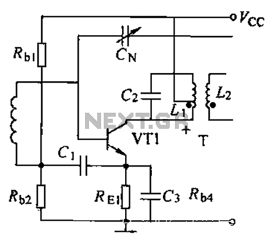
Common intermediate frequency amplifier circuit having a circuit and on the radio
A common intermediate frequency amplifier circuit is presented, along with its components and parameters. The reference values for the components are as follows: 1) Transistors: VT1 to 3DG19, Vcc = 6V. 2) Resistance values: R1 = 50 kΩ, R2 =...
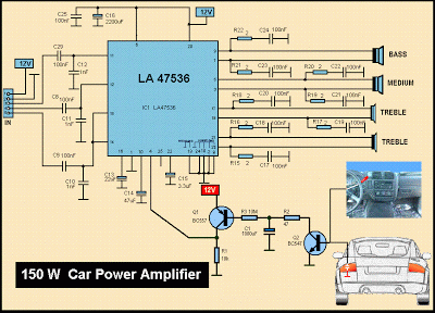
Schematic MP3 Car Audio Power AmplifierCircuits
This is a diagram of a car audio active loudspeaker utilizing the LF353 operational amplifier from National Semiconductor. For optimal performance, the NE5532 is recommended to split the audio signal into three frequency bands using an active filter. The SANYO...
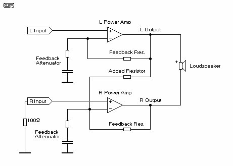
Amplifier Bridging
The primary advantage of this method of bridging is that no additional components are needed, which means that it is cheap, and there is no signal degradation from additional opamps in the circuit path. The results are at least as...
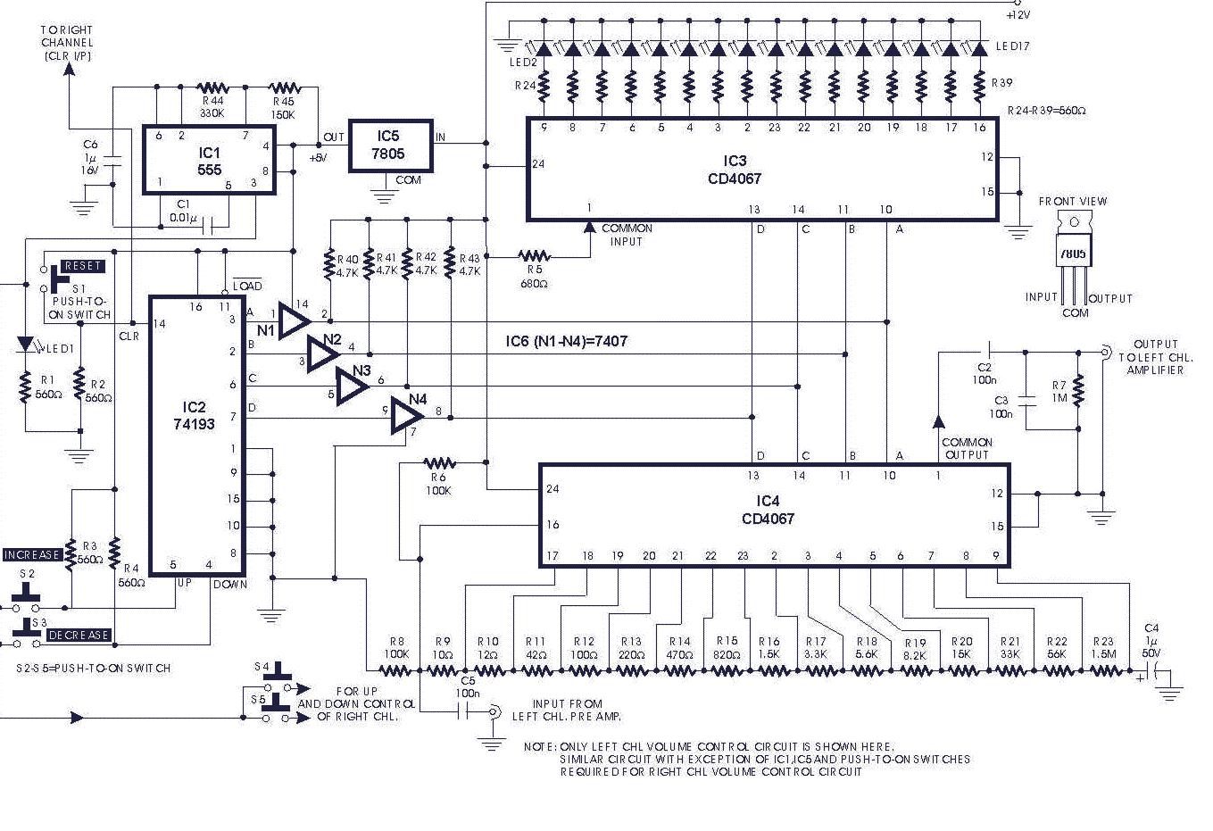
audio circuits 20
The gain of the single-stage virtual earth amplifier IC1 is determined by the drain-source resistance of the field-effect transistor (FET). Resistors R1, R2, and R3 linearize the FET's voltage-current characteristic. A control voltage is derived from the output signal using...
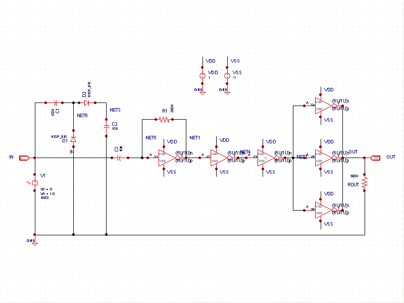
Sine to Square Wave Converter
This schematic example demonstrates a sinusoidal voltage input at a frequency of 10 kHz, which is converted to a square wave using an inverter-based circuit. The VDD and VSS rails are connected to +1V and -1V, respectively. The control file...
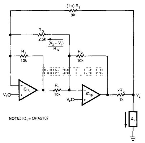
Bootstrapped Amp Current Source
This circuit responds to the difference between Vj and V2. Rq sets the gain. Resistors XR2 and (1 - X) R2 produce the bootstrap effect. These two resistors convert the circuit's output voltage to a current. IC1 and IC2 are...