


Test circuit diagram with feedback factor of 1 83 of TDA6120Q
#TDA6120Q
#feedback factor
#test circuit
#input signal
#operational amplifier
#circuit diagram
#feedback network
#electronics testing
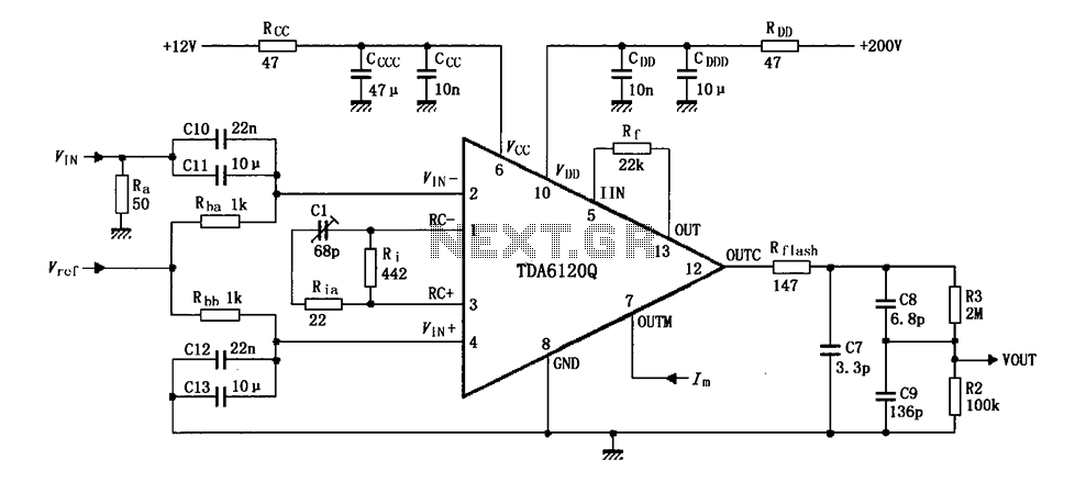
Description: Feedback has indicated that the TDA6120Q test circuit, as shown in the figure, utilizes an input signal (Vi) composed of resistors Ra and capacitors C10 and C11, which are fed into the TDA6120Q at pins 2, 3, and 4. These pins serve as the inverting and non-inverting input terminals of the differential input stage. The amplified signal exits from pin 12 and is processed through the network formed by resistors Rflash, R2, R3, and capacitors C7, C8, and C9. The feedback network is established by the resistor connected to pin 13 (Rf), which enhances the output's dynamic range. Additionally, the resistors connected to pins 1 and 3 (Ri and Rin) and capacitor C1 create a pre-emphasis network. The output stage includes a resistor (Rflash) that provides cathode discharge protection, limiting current and voltage during high-voltage discharges. Decoupling capacitors must be added to Vcc (pin 6) and VDD (pin 10), with high-frequency ceramic capacitors and electrolytic capacitors connected in parallel for optimal performance.
The TDA6120Q is a versatile integrated circuit designed for use in various audio and video applications. It features a differential input stage that effectively amplifies the input signal while maintaining low noise levels. The configuration of resistors and capacitors in the circuit plays a crucial role in shaping the signal and ensuring stability.
The input stage, consisting of Ra, C10, and C11, serves to filter and condition the incoming signal before it reaches the differential inputs. This is critical for achieving high fidelity in the output. The differential inputs at pins 2 and 3 allow for common-mode noise rejection, enhancing the overall signal integrity.
The amplified output from pin 12 is further processed through a network of resistors and capacitors, which serve to adjust the frequency response and gain of the circuit. The feedback resistor (Rf) connected to pin 13 is integral to maintaining stability and controlling the gain of the amplifier, allowing for dynamic range expansion in the output signal.
The pre-emphasis network, formed by Ri, Rin, and C1, is essential for compensating for signal losses at higher frequencies, ensuring that the output maintains clarity and detail. This network is particularly important in applications where signal degradation may occur due to transmission over long distances.
The inclusion of Rflash at the output provides critical protection against voltage spikes, which can occur during sudden changes in load or external disturbances. This resistor limits the current and protects the circuit from potential damage, thereby enhancing the reliability of the system.
For proper operation, it is essential to include decoupling capacitors at Vcc and VDD. The use of both ceramic and electrolytic capacitors in parallel ensures that the circuit is adequately decoupled across a wide frequency range, minimizing the risk of oscillations and ensuring stable operation under varying load conditions. This design consideration is vital for maintaining the performance of the TDA6120Q in real-world applications.Feedback has shown TDA6120Q factor 1/83 test circuit shown in Figure. Input signal Vi composed by Ra, C10, C11 input into the network TDA6120Q 2 feet, 2 feet and 4 feet are ins ide the differential input stage inverting input terminal and non-inverting input, the amplified signal from 12 feet out, after by the Rflash, R2, R3, C7, C8, C9 network of output. Resistance between 13,5 feet Rf is the feedback network, the output from the expansion of the dynamic range of action.
Resistance between 1,3 feet Ri, Rin and capacitor C1 constitute a pre-emphasis network. The output end of the resistor Rflash cathode discharge protection, when a high voltage discharge, serves to limit the current and voltage limiting effect. Vcc (6 feet), VDD (10 feet) must be added decoupling capacitors, high-frequency decoupling capacitance characteristics of a good ceramic capacitors and electrolytic capacitors connected in parallel.
The TDA6120Q is a versatile integrated circuit designed for use in various audio and video applications. It features a differential input stage that effectively amplifies the input signal while maintaining low noise levels. The configuration of resistors and capacitors in the circuit plays a crucial role in shaping the signal and ensuring stability.
The input stage, consisting of Ra, C10, and C11, serves to filter and condition the incoming signal before it reaches the differential inputs. This is critical for achieving high fidelity in the output. The differential inputs at pins 2 and 3 allow for common-mode noise rejection, enhancing the overall signal integrity.
The amplified output from pin 12 is further processed through a network of resistors and capacitors, which serve to adjust the frequency response and gain of the circuit. The feedback resistor (Rf) connected to pin 13 is integral to maintaining stability and controlling the gain of the amplifier, allowing for dynamic range expansion in the output signal.
The pre-emphasis network, formed by Ri, Rin, and C1, is essential for compensating for signal losses at higher frequencies, ensuring that the output maintains clarity and detail. This network is particularly important in applications where signal degradation may occur due to transmission over long distances.
The inclusion of Rflash at the output provides critical protection against voltage spikes, which can occur during sudden changes in load or external disturbances. This resistor limits the current and protects the circuit from potential damage, thereby enhancing the reliability of the system.
For proper operation, it is essential to include decoupling capacitors at Vcc and VDD. The use of both ceramic and electrolytic capacitors in parallel ensures that the circuit is adequately decoupled across a wide frequency range, minimizing the risk of oscillations and ensuring stable operation under varying load conditions. This design consideration is vital for maintaining the performance of the TDA6120Q in real-world applications.Feedback has shown TDA6120Q factor 1/83 test circuit shown in Figure. Input signal Vi composed by Ra, C10, C11 input into the network TDA6120Q 2 feet, 2 feet and 4 feet are ins ide the differential input stage inverting input terminal and non-inverting input, the amplified signal from 12 feet out, after by the Rflash, R2, R3, C7, C8, C9 network of output. Resistance between 13,5 feet Rf is the feedback network, the output from the expansion of the dynamic range of action.
Resistance between 1,3 feet Ri, Rin and capacitor C1 constitute a pre-emphasis network. The output end of the resistor Rflash cathode discharge protection, when a high voltage discharge, serves to limit the current and voltage limiting effect. Vcc (6 feet), VDD (10 feet) must be added decoupling capacitors, high-frequency decoupling capacitance characteristics of a good ceramic capacitors and electrolytic capacitors connected in parallel.
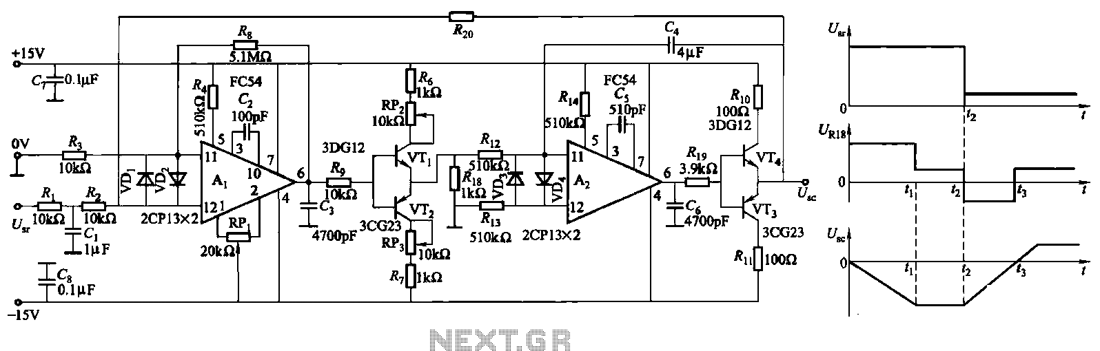
ZKJ-S-type buffer controller circuit
The ZKJ-S-type buffer controller circuit is designed for motor starting slip control. This buffer controller is composed of two operational amplifiers, Ai and Az. The operational amplifier Ai functions as a speed amplifier that saturates, while Az acts as an...
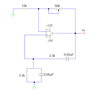
OP AMP SINE WAVE GENERATOR CIRCUIT
An operational amplifier-based sine wave generator circuit, commonly known as a Wien bridge oscillator, is recognized for its simplicity and stability. The Wien bridge oscillator connects the Wien bridge circuit between the amplifier's input and output terminals. The bridge features...
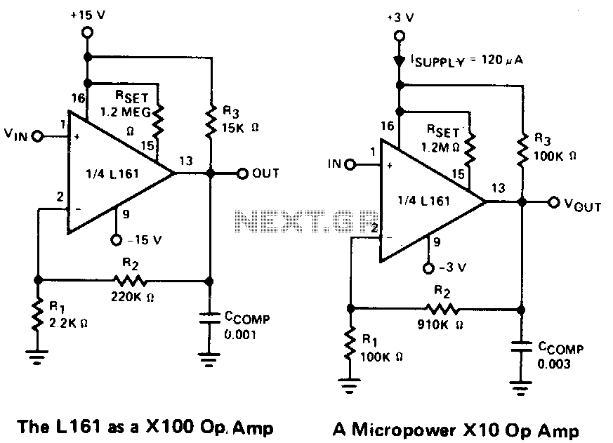
Operational-amplifiers
This is a single gain-of-100 amplifier with a gain-bandwidth product of 20 MHz. The primary limitation in performance is the low slew rate of 0.3 V/μs imposed by the charging of Ccomp. The effects of slew rate and compensation are...
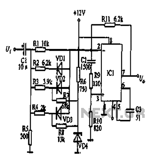
Square transform circuit diagram
At the input of the operational amplifier, a resistor-diode network can be constructed to create a square-law function conversion circuit. This resistor-diode network acts as a voltage divider, where the input voltage variations lead to different partial pressures. The three...
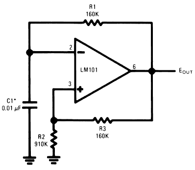
operational amplifier op amp oscillator
The timing capacitor (C1) generates multiple time constants, facilitating substantial voltage fluctuations at the input, attributable to the LM101's extensive input voltage range. It is advisable to decrease the value of resistor R2 and to increase the capacitance of C1...
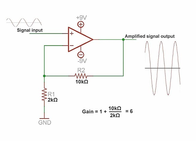
amplify voltage and build microphone circuit
An amplifier is a device that increases the voltage in a circuit. The simplest type is an operational amplifier, and this video will demonstrate how these devices function and how to implement them in electronic applications. As an example, you...
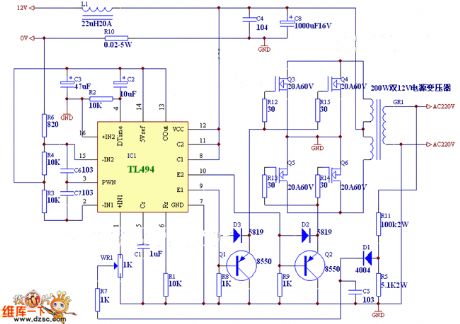
Precision current sink sourcel
An operational amplifier circuit can provide a constant voltage source with a high amplification factor and substantial load current. Even with significant variations in circuit parameters, the output voltage maintains high precision. The output current limit is managed by transistors...
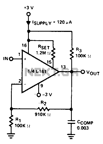
X10 operational amplifier
The amplifier is 3 dB down at 100 kHz and has a slew rate of 0.02 V/µs.
The amplifier's performance characteristics indicate that it experiences a 3 dB attenuation at a frequency of 100 kHz. This specification suggests that at this...
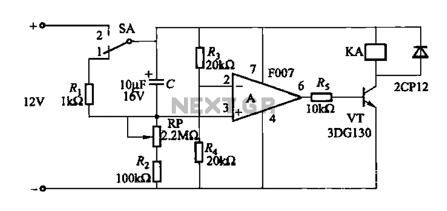
A delay circuit using an operational amplifier
A delay circuit utilizing an operational amplifier functions as a comparator, providing high timing accuracy. The timer's delay range is from 1 to 30 seconds. The delay time is determined by resistors Ri, RP, and capacitor C. By adjusting RP,...