


Track-and-hold
#track-and-hold
#op-amp
#FET switch
#TTL logic
#hold capacitor
#buffered output
#5-MHz
#voltage compensation
#signal processing
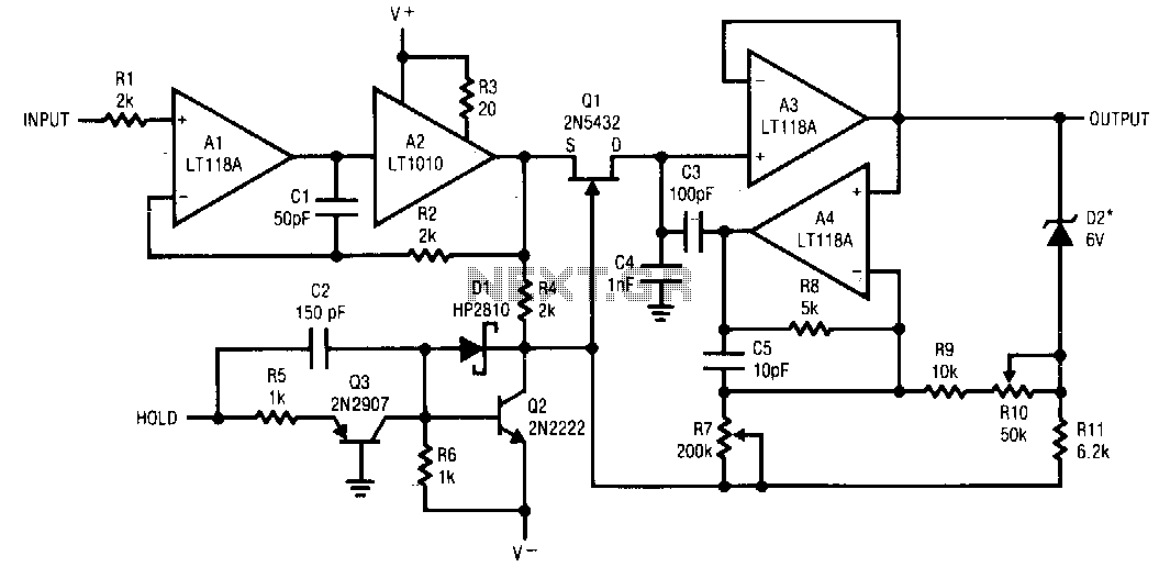
Description: The 5-MHz track and hold circuit operates with a 400-kHz power bandwidth, capable of driving ±10 V. A buffered input follower is used to drive the hold capacitor, C4, through Q1, which is a low-resistance FET switch. The positive hold command is supplied by TTL logic, with Q3 providing level shifting to the switch driver, Q2. The output is buffered by A3. When the gate is driven to V for hold, it extracts charge from the hold capacitor. A compensating charge is introduced into the hold capacitor through C3. The transition into hold mode is made independent of the input level using R7, and it can be adjusted to zero with R10. Since internal dissipation can be significant when driving fast signals into a capacitive load, it is recommended to use a buffer in a power package. Increasing the buffer quiescent current to 40 mA with R3 enhances frequency response.
The 5-MHz track and hold circuit is designed to accurately capture and maintain an analog voltage level for a specified duration. The circuit operates with a power bandwidth of 400 kHz, allowing it to effectively handle signals with fast transitions while maintaining a voltage output range of ±10 V.
At the core of the circuit is a buffered input follower, which ensures that the input signal is accurately tracked before it is stored. The hold capacitor, C4, is controlled by a low-resistance FET switch, Q1, which provides efficient charge transfer. The hold command is generated by TTL logic, which ensures reliable digital control of the analog signal. The level shifting of the command signal is managed by transistor Q3, which interfaces with the switch driver, Q2, ensuring that the FET switch operates correctly in response to the hold command.
The output stage of the circuit features an additional buffer, A3, which isolates the hold capacitor from the load, preventing any unwanted loading effects that could distort the output signal. When the gate of the FET switch is driven to the voltage level designated for hold, the switch opens, allowing the charge stored in C4 to be extracted. To maintain the integrity of the stored voltage, a compensating charge is added to C4 through capacitor C3, which helps to stabilize the output during the hold period.
The design incorporates resistors R7 and R10, which play critical roles in ensuring the transition into hold mode is independent of the input signal level. R7 allows for setting the threshold at which the hold operation occurs, while R10 provides a means to fine-tune this threshold to zero, ensuring precise control over the hold function.
Given the high internal dissipation that can occur when fast signals are being driven into a capacitive load, the circuit employs a buffer in a power package to manage thermal performance effectively. Increasing the quiescent current of the buffer to 40 mA via resistor R3 significantly enhances the frequency response of the circuit, allowing it to handle high-speed signals more effectively while minimizing distortion and maintaining signal fidelity. This design consideration is crucial for applications requiring high precision and reliability in analog signal processing.The 5-MHz track and hold shown here has a 400-kHz power bandwidth driving ±10 V. A buffered input follower drives the hold capacitor, C4, through Ql, a low resistance FET switch. The positive hold conuuand is supplied by TTL logic, with Q3Ievel shifting to the switch driver, Q2. The output is buffered by A3. When the gate is driven to V-for hold, it pulls the charge out of the hold capacitor. A compensating charge is put into the hold capacitor through C3. The step into hold is made independent of the input level with R7, and adjusted to zero with RIO. Since internal dissipation can be quite high when driving fast signals into a capacitive load, using a buffer in a power package is reconuuended. Raising the buffer quiescent current to 40 mA with R3 improves frequency response.
The 5-MHz track and hold circuit is designed to accurately capture and maintain an analog voltage level for a specified duration. The circuit operates with a power bandwidth of 400 kHz, allowing it to effectively handle signals with fast transitions while maintaining a voltage output range of ±10 V.
At the core of the circuit is a buffered input follower, which ensures that the input signal is accurately tracked before it is stored. The hold capacitor, C4, is controlled by a low-resistance FET switch, Q1, which provides efficient charge transfer. The hold command is generated by TTL logic, which ensures reliable digital control of the analog signal. The level shifting of the command signal is managed by transistor Q3, which interfaces with the switch driver, Q2, ensuring that the FET switch operates correctly in response to the hold command.
The output stage of the circuit features an additional buffer, A3, which isolates the hold capacitor from the load, preventing any unwanted loading effects that could distort the output signal. When the gate of the FET switch is driven to the voltage level designated for hold, the switch opens, allowing the charge stored in C4 to be extracted. To maintain the integrity of the stored voltage, a compensating charge is added to C4 through capacitor C3, which helps to stabilize the output during the hold period.
The design incorporates resistors R7 and R10, which play critical roles in ensuring the transition into hold mode is independent of the input signal level. R7 allows for setting the threshold at which the hold operation occurs, while R10 provides a means to fine-tune this threshold to zero, ensuring precise control over the hold function.
Given the high internal dissipation that can occur when fast signals are being driven into a capacitive load, the circuit employs a buffer in a power package to manage thermal performance effectively. Increasing the quiescent current of the buffer to 40 mA via resistor R3 significantly enhances the frequency response of the circuit, allowing it to handle high-speed signals more effectively while minimizing distortion and maintaining signal fidelity. This design consideration is crucial for applications requiring high precision and reliability in analog signal processing.The 5-MHz track and hold shown here has a 400-kHz power bandwidth driving ±10 V. A buffered input follower drives the hold capacitor, C4, through Ql, a low resistance FET switch. The positive hold conuuand is supplied by TTL logic, with Q3Ievel shifting to the switch driver, Q2. The output is buffered by A3. When the gate is driven to V-for hold, it pulls the charge out of the hold capacitor. A compensating charge is put into the hold capacitor through C3. The step into hold is made independent of the input level with R7, and adjusted to zero with RIO. Since internal dissipation can be quite high when driving fast signals into a capacitive load, using a buffer in a power package is reconuuended. Raising the buffer quiescent current to 40 mA with R3 improves frequency response.
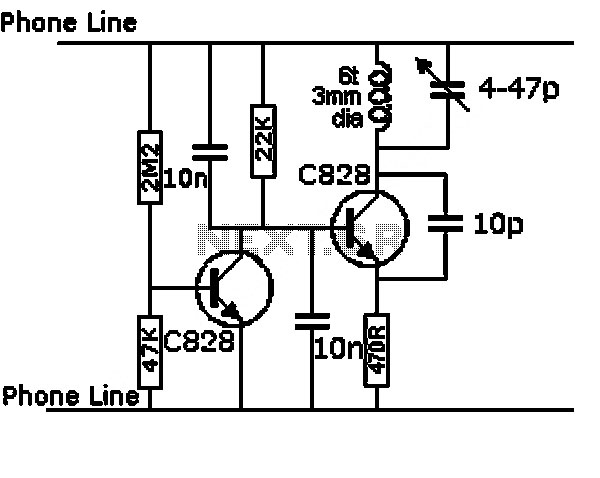
op amp based sound detector circuit
This circuit is designed for sound detection and generates an output signal when sound is detected. This output can trigger another circuit that activates an alarm, making it suitable for security applications. The circuit employs a condenser microphone to capture...
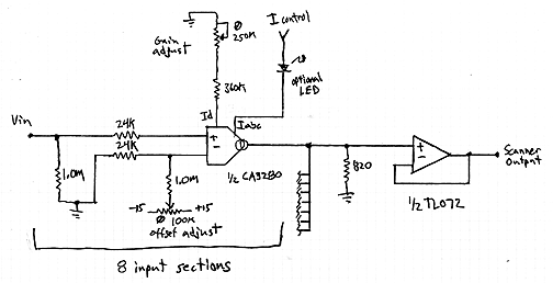
Interpolating Scanner Circuit
This design is for an interpolating scanner, a circuit featuring multiple signal inputs, a control voltage input, and a signal output. The output selectively transitions between inputs, smoothly fading from one to the next as the control voltage increases. A...
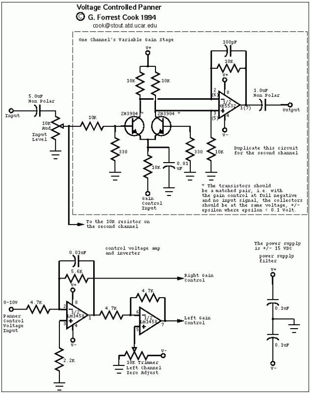
Voltage Controlled Panner
The control voltage is fed into the first half of a 1458 op-amp, this stage inverts the signal and sets the offset and gain for the right channel gain control circuit. This signal is then fed into the second half...
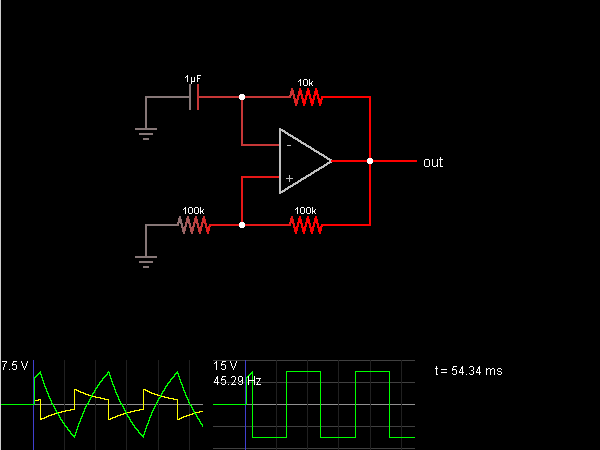
Relaxation Oscillator
This circuit is an oscillator that generates a square wave. The operational amplifier (op-amp) begins with its two inputs in an undefined state, starting with the non-inverting input slightly higher than the inverting input. The op-amp significantly amplifies this difference,...
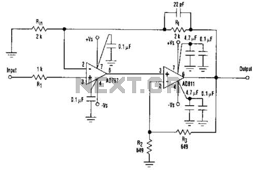
Fast Composite Amplifier Circuit
An ultra-low-noise, low-distortion operational amplifier, the AD797, is combined with the ADS 11 operational amplifier, which provides high bandwidth and a 100-mA output drive capability. This composite amplifier circuit is effective for driving high-resolution ADCs and ATE systems. The fast...
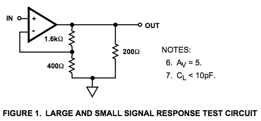
op amp Why the resistor in this op-amp circuit
Here is a circuit diagram for a signal response test circuit from the specification sheet for a HA-5195 operational amplifier. It appears to be a non-inverting amplifier circuit with a gain of 5, along with a 200-ohm resistor connecting Vout...
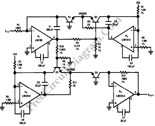
Power Function Circuit
It is possible to easily generate various non-linear functions such as X^(1/2), X^2, X^3, 1/X, XY, and X/Y using logarithms. In this context, division is transformed into subtraction, while multiplication is converted into addition.
The application of logarithmic properties in electronic...
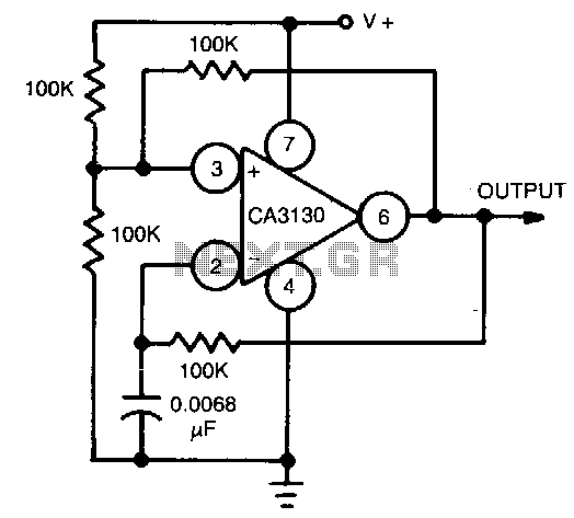
Classic-op-amp-astable-multivibrator
This circuit utilizes the CA3130 BiMOS operational amplifier, which operates at a frequency of 1 kHz. It features a rail-to-rail output swing, ensuring that the output can reach the supply voltage levels. The frequency of operation remains independent of supply...
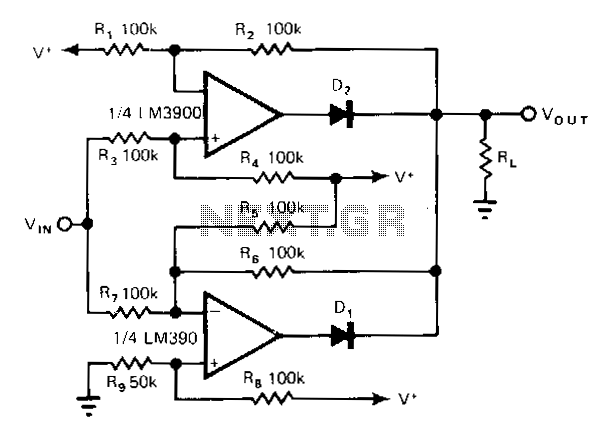
Norton-amplifier
The non-inverting amplifier has a gain of R2/R3 (1 in this case) and produces a voltage of V during a positive excursion of Vin with respect to ground. The inverting amplifier accommodates the negative excursions of V; its gain is...