


Units from the MAX4100 4101 gain buffer circuit diagram
#MAX4100
#MAX4101
#unit gain buffer
#feedback loop
#amplifier
#small resistor
#circuit diagram
#buffer circuit
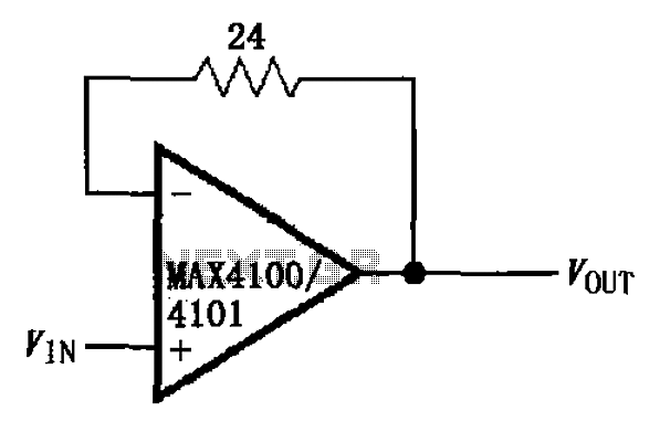
Description: The circuit illustrated is a unit gain buffer circuit utilizing the MAX4100/4101 operational amplifiers. It incorporates a small resistor (24 ohms) within the feedback loop of the amplifier, thereby establishing a unity gain buffer. This configuration maximizes the bandwidth of the circuit while minimizing overshoot and optimizing settling time. Additionally, the resistor mitigates the adverse effects of parasitic inductance and capacitance, enhancing the stability of the circuit and reducing errors attributed to the input bias current. The output voltage (VOUT) is equal to the input voltage (VIN).
The MAX4100/4101 unit gain buffer circuit is designed to provide high-speed signal buffering with minimal distortion. The operational amplifiers in this configuration are known for their low input offset voltage and high slew rate, making them suitable for applications requiring fast response times. The inclusion of a 24-ohm feedback resistor is a strategic choice; it balances the need for stability against the potential for increased noise and distortion.
In this circuit, the feedback resistor serves multiple purposes. Primarily, it helps to control the gain of the amplifier, ensuring that the output remains a faithful reproduction of the input signal without amplification or attenuation. This is crucial in applications such as signal conditioning, where preserving the integrity of the signal is paramount.
Moreover, the resistor's presence in the feedback loop aids in dampening oscillations that may arise from the inherent capacitance and inductance present in the circuit. By providing a controlled path for feedback, the resistor stabilizes the operational amplifier's response, allowing for a fast settling time that is essential in high-speed applications.
The characteristics of the MAX4100/4101 make them ideal for use in a variety of electronic applications, including audio processing, sensor signal buffering, and data acquisition systems. The unit gain buffer configuration ensures that the circuit can drive capacitive loads effectively, making it suitable for interfacing with other stages of a signal processing chain without introducing significant phase shifts or delays.
Overall, this unit gain buffer circuit exemplifies effective design principles in electronic engineering, focusing on stability, speed, and signal integrity, which are critical for modern high-performance electronics. As shown by FIG MAX4100/4101 unit gain buffer circuit constituted. This circuit uses a small resistor (24 ) placed in the feedback loop amplifier constituting a unity gain buff er, so the maximum bandwidth of the circuit, and has a low overshoot and fast settling time; at the same time this resistance can inhibit parasitic inductance and capacitance of the negative influence the stability of the circuit best, it can also reduce the error caused by the input bias current. VOUT VIN.
The MAX4100/4101 unit gain buffer circuit is designed to provide high-speed signal buffering with minimal distortion. The operational amplifiers in this configuration are known for their low input offset voltage and high slew rate, making them suitable for applications requiring fast response times. The inclusion of a 24-ohm feedback resistor is a strategic choice; it balances the need for stability against the potential for increased noise and distortion.
In this circuit, the feedback resistor serves multiple purposes. Primarily, it helps to control the gain of the amplifier, ensuring that the output remains a faithful reproduction of the input signal without amplification or attenuation. This is crucial in applications such as signal conditioning, where preserving the integrity of the signal is paramount.
Moreover, the resistor's presence in the feedback loop aids in dampening oscillations that may arise from the inherent capacitance and inductance present in the circuit. By providing a controlled path for feedback, the resistor stabilizes the operational amplifier's response, allowing for a fast settling time that is essential in high-speed applications.
The characteristics of the MAX4100/4101 make them ideal for use in a variety of electronic applications, including audio processing, sensor signal buffering, and data acquisition systems. The unit gain buffer configuration ensures that the circuit can drive capacitive loads effectively, making it suitable for interfacing with other stages of a signal processing chain without introducing significant phase shifts or delays.
Overall, this unit gain buffer circuit exemplifies effective design principles in electronic engineering, focusing on stability, speed, and signal integrity, which are critical for modern high-performance electronics. As shown by FIG MAX4100/4101 unit gain buffer circuit constituted. This circuit uses a small resistor (24 ) placed in the feedback loop amplifier constituting a unity gain buff er, so the maximum bandwidth of the circuit, and has a low overshoot and fast settling time; at the same time this resistance can inhibit parasitic inductance and capacitance of the negative influence the stability of the circuit best, it can also reduce the error caused by the input bias current. VOUT VIN.
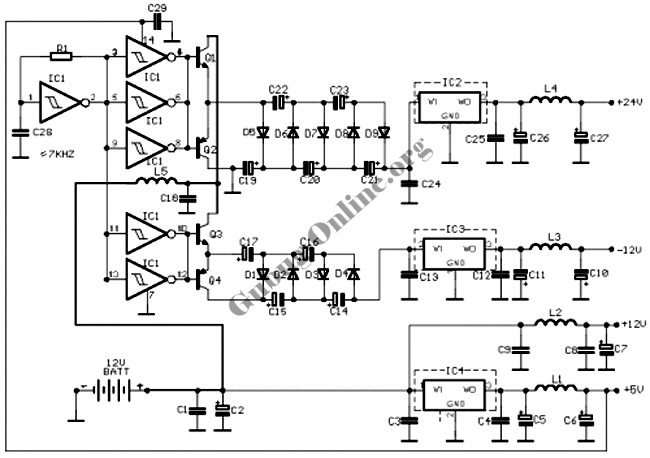
DC-Coupled Audio Amplifier Circuit
This design circuit for audio amplifiers with DC coupling to the load is not commonly used today, despite its clear advantages. One advantage is the elimination of the need for a second (symmetric) power supply, and another is the improved...
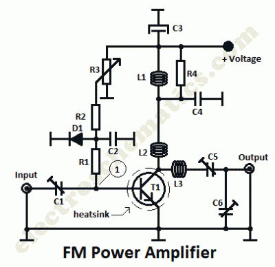
Radio Amplifiers Circuits
This is a 1 watt FM amplifier with a robust design that can be used to amplify an RF signal in the 88 to 108 MHz band. It is highly sensitive when utilizing quality RF power amplifier transistors, trimmers, and...
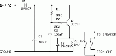
Amplifier Output Delay with Relay Schematic Diagram
This is a minimal circuit designed for individual audio amplifier projects to control the presenter output relay. The purpose of this circuit is to manage the relay that activates the speaker output within the audio amplifier. The circuit introduces a...
audio amp
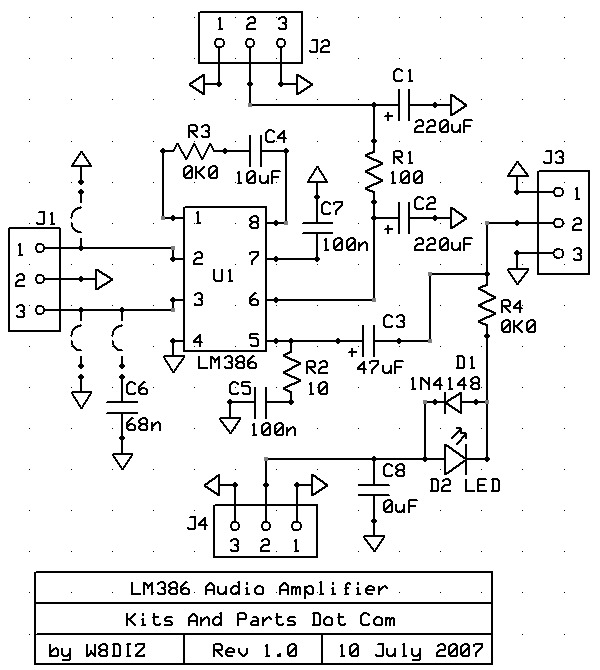
Install the red LED at D2. Align the flat side of the LED with the PCB outline. Install a jumper wire at R4 and install a 220µF electrolytic capacitor at C8 with the negative side connected to ground. Connect pin...
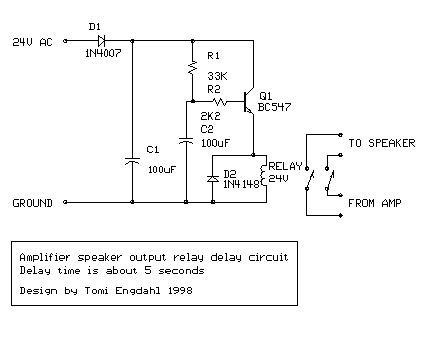
Amplifier Circuit Output Relay Delay Audio
This is a simple circuit designed for an audio amplifier project to control the speaker output relay. The purpose of this circuit is to manage the relay that activates the speaker output in the audio amplifier. The circuit is designed...
Stabilized-amplifier
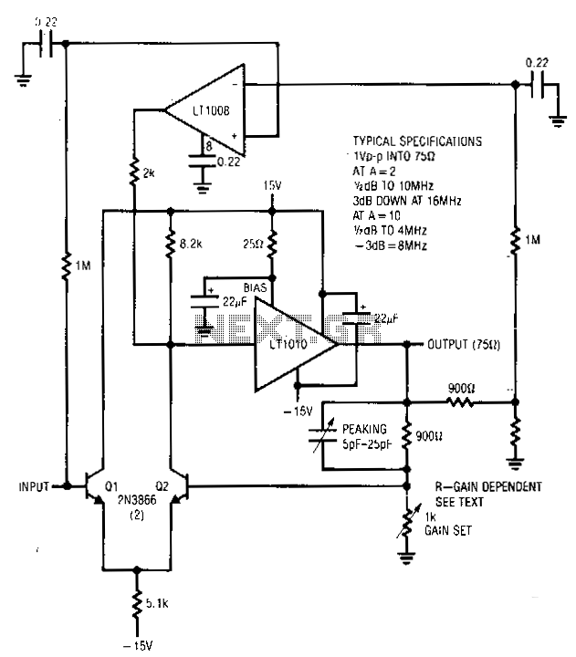
This amplifier operates across a broad range of gains, typically from 1 to 10. It integrates the LT1010 with a fast discrete stage and an LT1008-based destabilizing loop. Transistors Q1 and Q2 create a differential stage that converts to a...

Amplifier Timer Circuit
This circuit turns off an amplifier or any other device when a low-level audio signal fed to its input is absent for at least 15 minutes. By pressing P1, the device is powered on, supplying power to any appliance connected...
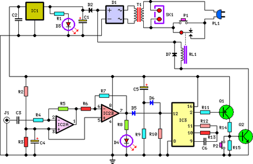
Amplifier Timer Circuit Schematic
This circuit deactivates an amplifier or any connected device when a low-level audio signal at its input is absent for at least 15 minutes. Pressing P1 turns the device on, supplying power to any appliance connected to SK1. The input...
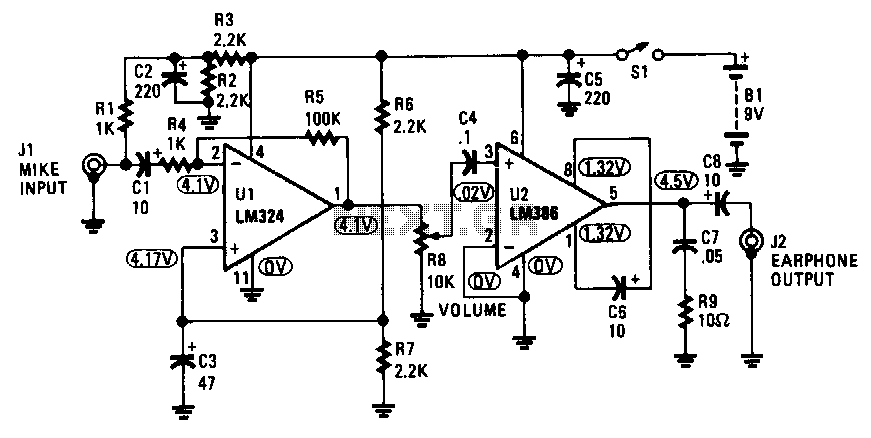
Tv-audio-amplifier
The amplifier captures the audio output signal from the TV and amplifies it to drive a set of earphones for private listening. It is constructed using an LM324 quad operational amplifier and an LM386 low-power audio amplifier. The circuit employs...