


Zero crossing detector
#zero crossing detector
#op-amp
#sine wave
#A/D converter
#input offset
#microvolts
#squaring circuit
#nulling voltage
#accuracy
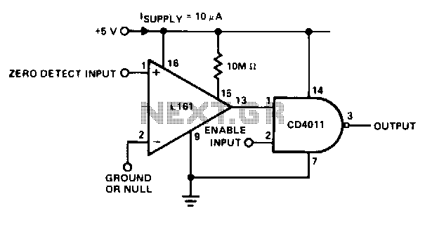
Description: This detector is useful in sine wave squaring circuits and A/D converters. The positive input may either be grounded or connected to a nulling voltage that cancels input offsets and enables accuracy to within microvolts of ground. The CMOS output will switch to within a few millivolts of either rail for an input voltage change of less than 200 µV.
The described detector serves a critical role in applications involving sine wave squaring circuits and analog-to-digital (A/D) converters. Its functionality is primarily based on its ability to handle input offsets effectively, which is crucial for maintaining precision in high-resolution applications. The detector features a positive input that can be either grounded or connected to a nulling voltage. This nulling voltage is essential for compensating any inherent input offsets, thereby enhancing the accuracy of the measurements to within microvolt levels relative to ground.
In terms of performance, the CMOS output of the detector is designed to switch within a few millivolts of the supply rails, which signifies its capability to respond accurately to minor changes in input voltage. Specifically, it has a sensitivity threshold that allows it to detect input voltage variations of less than 200 µV. This high level of sensitivity is particularly advantageous in applications where precise voltage levels must be monitored or converted, such as in signal processing and digital data acquisition systems.
The integration of this detector into a circuit can significantly improve the overall performance of sine wave squaring and A/D conversion processes by ensuring that the output reflects the true characteristics of the input signal. This is especially important in high-frequency applications where signal integrity must be preserved. The ability to maintain accuracy in the presence of input offsets and minor voltage fluctuations makes this detector a valuable component in modern electronic design.This detector is useful in sine wave squaring circuits and A/D converters. The positive input may either be grounded or con-output nected a nulling voltage which cancels input offsets and enables accuracy to within microvolts of ground The CMOS output will switch to within a few millivolts of either rail for an input voltage change of less than 200 µV.
The described detector serves a critical role in applications involving sine wave squaring circuits and analog-to-digital (A/D) converters. Its functionality is primarily based on its ability to handle input offsets effectively, which is crucial for maintaining precision in high-resolution applications. The detector features a positive input that can be either grounded or connected to a nulling voltage. This nulling voltage is essential for compensating any inherent input offsets, thereby enhancing the accuracy of the measurements to within microvolt levels relative to ground.
In terms of performance, the CMOS output of the detector is designed to switch within a few millivolts of the supply rails, which signifies its capability to respond accurately to minor changes in input voltage. Specifically, it has a sensitivity threshold that allows it to detect input voltage variations of less than 200 µV. This high level of sensitivity is particularly advantageous in applications where precise voltage levels must be monitored or converted, such as in signal processing and digital data acquisition systems.
The integration of this detector into a circuit can significantly improve the overall performance of sine wave squaring and A/D conversion processes by ensuring that the output reflects the true characteristics of the input signal. This is especially important in high-frequency applications where signal integrity must be preserved. The ability to maintain accuracy in the presence of input offsets and minor voltage fluctuations makes this detector a valuable component in modern electronic design.This detector is useful in sine wave squaring circuits and A/D converters. The positive input may either be grounded or con-output nected a nulling voltage which cancels input offsets and enables accuracy to within microvolts of ground The CMOS output will switch to within a few millivolts of either rail for an input voltage change of less than 200 µV.
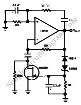
Wien Bridge Sine Wave Oscillator
Achieving the appropriate amplifier loop gain is a significant challenge in generating a low distortion, constant amplitude sine wave. Nevertheless, this issue can be addressed with...
Amplifier loop gain is a critical parameter in the design of audio and signal processing...
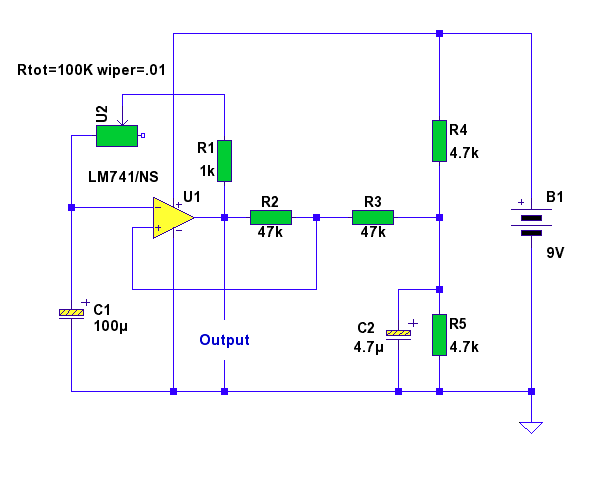
741 Astable Timer
In this circuit, a standard operational amplifier (op-amp) is configured as an astable multivibrator. The output is non-symmetrical, but it has the advantage of being controlled by only one resistor and one capacitor: a 100k variable resistor (U2) and a...
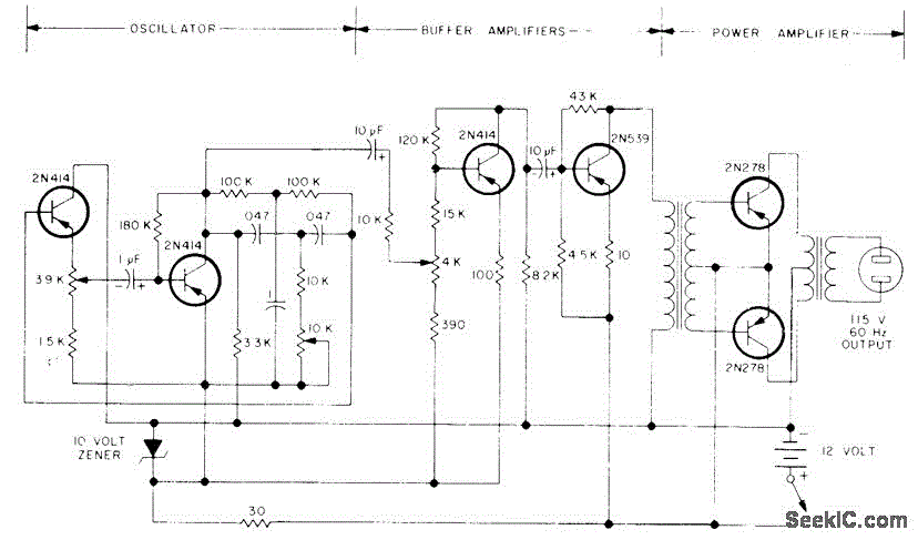
100W SINE AT 60Hz
The circuit primarily comprises a 60-Hz sine-wave oscillator featuring a 10K frequency-control potentiometer, two buffering stages, and a push-pull power amplifier. This design effectively addresses the noise issues associated with square-wave inverters, particularly when powering a 115-V radio receiver or...
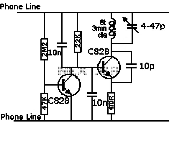
tuned sine wave oscillator circuit
This design circuit functions as a sine wave oscillator, providing both sine and square wave outputs across a frequency range from below 20 Hz to above 20 KHz. The oscillation frequency can be easily adjusted by varying a single resistor....
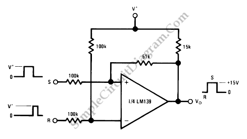
Bi-Stable Multivibrator (RS Flip-FLop) with Op-Amp
This bi-stable circuit utilizes an operational amplifier and functions similarly to an RS flip-flop. A bi-stable circuit is characterized by having two stable states: low and high, remaining in the low state until it is set to high.
The bi-stable circuit...
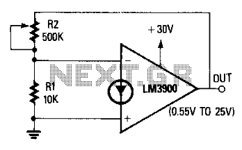
Variable-Voltage Reference Source
The non-inverting terminal of the operational amplifier (op-amp) is grounded, and the circuit utilizes the voltage at the inverting terminal as a reference. The voltage gain of the circuit is determined by the ratio of resistors R2 to R. When...
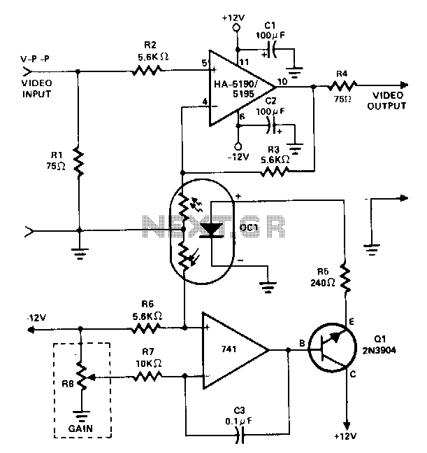
Dc-gain-controlled-video-amplifier
This amplifier utilizes a cascaded operational amplifier (op amp) integrator and a transistor buffer, Q1, to drive the gain control element. With a minor modification, the HA-5190/5195 stage is configured as a conventional non-inverting op amp and includes input and...
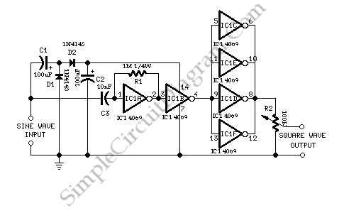
Self Powered Sine Wave to Square Converter
This circuit utilizes a single active component, the 4069 IC, to convert sine waves into square waves without requiring an external power source. It is designed for testing audio instruments.
The circuit leverages the characteristics of the 4069 IC, which is...
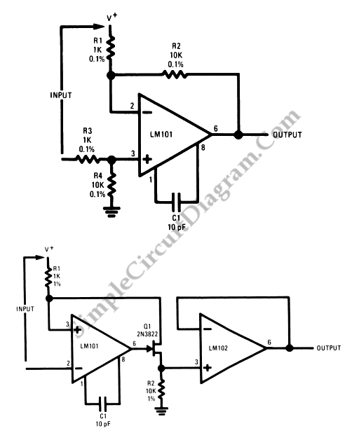
Op-Amp Application: Level Shifting Amplifier
In linear equipment design, it is sometimes necessary to take a voltage that is referenced to a certain DC level and generate an amplified output that is also referenced.
In linear circuit design, the process of amplifying a voltage that is...