


Local Oscillator Stage
#Si570
#frequency setting
#CMOS
#LVDS
#voltage check
#programming
#component variations
#current draw
#local oscillator
#dc voltages
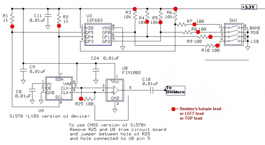
Description: The current draw should be between 80 and 100 mA. The exact value is highly dependent on the Si570, its version (CMOS vs. LVDS), the frequency setting, and variations in the circuit components. The SW1 programming of U3 can be tested by measuring the DC voltages at pins 1 through 7. Pins 1 through 3 should consistently show approximately 3.27 VDC. The voltages at pins 4 through 7 will vary based on the corresponding dip switch settings (pins 4 through 7 correspond to dip switches 1 through 4).
The described circuit operates within a current range of 80 to 100 mA, which is crucial for ensuring the proper functionality of the Si570 frequency generator. The Si570 can be configured in different versions, namely CMOS or LVDS, each affecting the current draw due to inherent differences in their electrical characteristics. The frequency setting also plays a significant role, as it can influence the load on the circuit and, consequently, the current consumption.
To assess the programming of the SW1 switch associated with the U3 component, voltage measurements should be taken at pins 1 through 7. It is expected that pins 1 to 3 maintain a stable DC voltage of approximately 3.27 VDC, indicating that the power supply and initial circuit conditions are functioning as intended. The voltages present at pins 4 through 7 will fluctuate based on the settings of the corresponding dip switches, which are critical for configuring the operational parameters of the circuit. Each dip switch setting alters the behavior of the circuit, allowing for flexibility in operation and performance.
In summary, careful monitoring of the current draw, along with the appropriate voltage levels at the designated pins, is essential for verifying the functionality and reliability of the circuit involving the Si570 frequency generator.The current draw should be somewhere between 80 and 100 mA. The exact value is very much dependent upon the Si570, the version (CMOS vs LVDS), the frequency setting, and component variations in the circuit. You can test the SW1 programming of U3 by checking the dc voltages at pins 1 thru 7. Pins 1 thru 3 should always be approximately 3. 27 Vdc. Vo ltages at pins 4 thru 7 will vary, depending upon their corresponding dip switch settings (pins 4 thru 7 correspond to dip switches 1 thru 4):.
The described circuit operates within a current range of 80 to 100 mA, which is crucial for ensuring the proper functionality of the Si570 frequency generator. The Si570 can be configured in different versions, namely CMOS or LVDS, each affecting the current draw due to inherent differences in their electrical characteristics. The frequency setting also plays a significant role, as it can influence the load on the circuit and, consequently, the current consumption.
To assess the programming of the SW1 switch associated with the U3 component, voltage measurements should be taken at pins 1 through 7. It is expected that pins 1 to 3 maintain a stable DC voltage of approximately 3.27 VDC, indicating that the power supply and initial circuit conditions are functioning as intended. The voltages present at pins 4 through 7 will fluctuate based on the settings of the corresponding dip switches, which are critical for configuring the operational parameters of the circuit. Each dip switch setting alters the behavior of the circuit, allowing for flexibility in operation and performance.
In summary, careful monitoring of the current draw, along with the appropriate voltage levels at the designated pins, is essential for verifying the functionality and reliability of the circuit involving the Si570 frequency generator.The current draw should be somewhere between 80 and 100 mA. The exact value is very much dependent upon the Si570, the version (CMOS vs LVDS), the frequency setting, and component variations in the circuit. You can test the SW1 programming of U3 by checking the dc voltages at pins 1 thru 7. Pins 1 thru 3 should always be approximately 3. 27 Vdc. Vo ltages at pins 4 thru 7 will vary, depending upon their corresponding dip switch settings (pins 4 thru 7 correspond to dip switches 1 thru 4):.
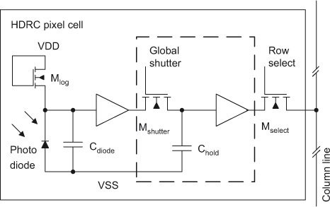
High dynamic range CMOS (HDRC) imagers for safety systems
The initial section of this document outlines the high dynamic range CMOS (HDRC) imager, a specialized type of CMOS image sensor characterized by its logarithmic response. The significant capabilities of high dynamic range (HDR) image acquisition are explained through mathematical...
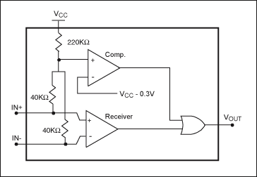
Understanding LVDS Fail-Safe Circuits
The LVDS receiver requires a failsafe function to prevent an uncertain output state in the event of an improper connection. This application note explores the circuits and characteristics of three common failsafe functions: external biasing, in-path, and parallel.
The LVDS (Low-Voltage...
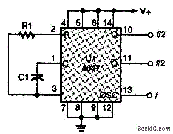
CD4047 CMOS OSCILLATOR
This CMOS square-wave oscillator utilizes the 4047 multivibrator circuit, suitable for both monostable (one-shot) and astable applications. In the provided configuration, the 4047 operates as an astable multivibrator. The circuit features three outputs from the 4047, with the first being...
CD4047 CMOS OSCILLATOR
This CMOS square-wave oscillator utilizes the 4047 multivibrator circuit, suitable for both monostable (one-shot) and astable applications. In the provided configuration, the 4047 operates as an astable multivibrator. The circuit features three outputs from the 4047, with the first being...
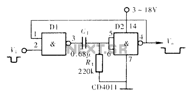
Monostable flip-flop circuit consisting of door
A CMOS NAND gate or NOR gate can form a monostable multivibrator, commonly referred to as a single-shot. This circuit is extensively used to delay pulse signals, allowing for signal stretching and shaping. The main principle involves utilizing the threshold...
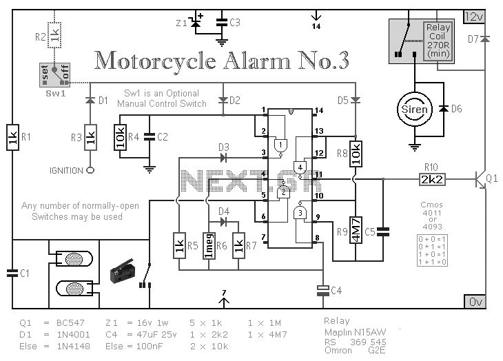
A Cmos Based Motorcycle Alarm
A CMOS-based motorcycle alarm circuit that features an intermittent siren output and automatic reset. It can be operated manually using a key switch or a hidden switch, and it can also be wired to set itself automatically.
The CMOS-based motorcycle alarm...
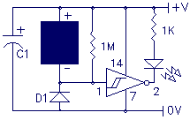
Wilf Rigter`s SIMD1 V1
Normally the active high output from the inverter is used to enable the remainder of the CMOS gates which then perform some useful function. When the SIMD1 triggers at night, it snaps on and the output signal can be used...
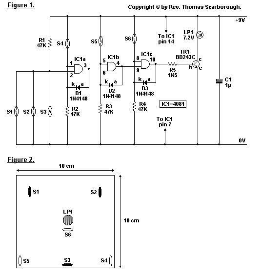
Magic Wand Conjuring Trick
The operation of the circuit is fairly simple. Three AND logic gates of a 4081 CMOS IC are employed, with gates IC1a to IC1c being configured as a standard cascaded latch circuit. S1 to S3 serve as reset switches. The...
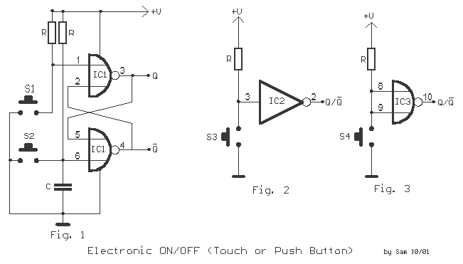
Electronic Switch ON-OFF
Here we have three choices, with which we can make electronic switches that use our touch or pressing (push button). We thus exploit the very big resistance of entry, that present the gates CMOS. In the fig.1 we have two...