


Voltage Controlled Oscillator using NE555
#NE555
#voltage-controlled oscillator
#voltage-to-frequency converter
#frequency modulation
#input voltage control

Description: A voltage-controlled oscillator using the NE555. This circuit is commonly referred to as a voltage-to-frequency converter because the output frequency is altered by varying the input voltage. As previously noted, pin 5 serves as the voltage control terminal, which is responsible for managing the edge and trigger levels. Typically, the control voltage is set at +2/3 VCC due to the internal voltage divider. However, an external voltage may be applied directly to this terminal or through a potentiometer, as shown in the accompanying figure. By adjusting the potentiometer, the control voltage can be varied. The voltage across the timing capacitor, which fluctuates between +Vcontrol and ½ Vcontrol, is also illustrated in the figure. When the control voltage is increased, the capacitor takes longer to charge and discharge, resulting in a decrease in frequency. Thus, the frequency is modified by changing the control voltage. The control voltage can be generated through a potentiometer or may originate from a transistor circuit, operational amplifier, or another device.
The NE555 timer is a versatile integrated circuit widely used in various applications, including oscillators, timers, and pulse generation. In the context of a voltage-controlled oscillator (VCO), the NE555 can be configured in astable mode, allowing it to generate a continuous square wave output whose frequency is dependent on the voltage applied at pin 5.
The circuit typically consists of the NE555 timer, a timing capacitor (C1), two resistors (R1 and R2), and a potentiometer (P1) to adjust the control voltage. The resistors R1 and R2 form a voltage divider that sets the threshold levels for the NE555. The timing capacitor C1 determines the charge and discharge time, which directly influences the output frequency.
When a voltage is applied to pin 5, the internal voltage divider of the NE555 adjusts the timing intervals based on the control voltage. The relationship between the control voltage and the output frequency is inversely proportional; as the control voltage increases, the frequency decreases due to the longer charge and discharge times of the capacitor.
It is essential to select appropriate values for R1, R2, and C1 to achieve the desired frequency range. The output frequency (f) can be calculated using the formula:
\[ f = \frac{1.44}{(R1 + 2R2) \times C1} \]
In this configuration, the potentiometer allows fine-tuning of the control voltage, facilitating precise frequency modulation. The output from the NE555 can be utilized to drive loads directly or can be fed into subsequent stages of a circuit, such as filters or amplifiers, depending on the application requirements.
This voltage-controlled oscillator circuit is particularly useful in applications requiring frequency modulation, such as in communication systems, signal generators, and audio synthesis, where varying the frequency in response to an input control voltage is necessary.A voltage-controlled oscillator using NE555 The circuit is usually known as a voltage-to-frequency converter as a result of the output frequency will be modified by changing the input voltage. As mentioned in previous blog posts, pin 5 terminal is voltage control terminal and its function is to manage the edge and trigger levels.
Normally, the con trol voltage is +2/3VCC because of the inner voltage divider. However, an external voltage will be applied to the current terminal directly or through a pot, as illustrated in figure, and by adjusting the pot, control voltage can be varied. Voltage across the timing capacitor is depicted in figure, that varies between +Vcontrol and ½ Vcontrol.
If control voltage is increased, the capacitor takes a extended to charge and discharge; the frequency, therefore, decreases. so the fre quency will be modified by changing the control volt age. Incidentally, the control voltage is also created offered through a pot, or it should be output of a transistor circuit, op-amp, or another device.
The NE555 timer is a versatile integrated circuit widely used in various applications, including oscillators, timers, and pulse generation. In the context of a voltage-controlled oscillator (VCO), the NE555 can be configured in astable mode, allowing it to generate a continuous square wave output whose frequency is dependent on the voltage applied at pin 5.
The circuit typically consists of the NE555 timer, a timing capacitor (C1), two resistors (R1 and R2), and a potentiometer (P1) to adjust the control voltage. The resistors R1 and R2 form a voltage divider that sets the threshold levels for the NE555. The timing capacitor C1 determines the charge and discharge time, which directly influences the output frequency.
When a voltage is applied to pin 5, the internal voltage divider of the NE555 adjusts the timing intervals based on the control voltage. The relationship between the control voltage and the output frequency is inversely proportional; as the control voltage increases, the frequency decreases due to the longer charge and discharge times of the capacitor.
It is essential to select appropriate values for R1, R2, and C1 to achieve the desired frequency range. The output frequency (f) can be calculated using the formula:
\[ f = \frac{1.44}{(R1 + 2R2) \times C1} \]
In this configuration, the potentiometer allows fine-tuning of the control voltage, facilitating precise frequency modulation. The output from the NE555 can be utilized to drive loads directly or can be fed into subsequent stages of a circuit, such as filters or amplifiers, depending on the application requirements.
This voltage-controlled oscillator circuit is particularly useful in applications requiring frequency modulation, such as in communication systems, signal generators, and audio synthesis, where varying the frequency in response to an input control voltage is necessary.A voltage-controlled oscillator using NE555 The circuit is usually known as a voltage-to-frequency converter as a result of the output frequency will be modified by changing the input voltage. As mentioned in previous blog posts, pin 5 terminal is voltage control terminal and its function is to manage the edge and trigger levels.
Normally, the con trol voltage is +2/3VCC because of the inner voltage divider. However, an external voltage will be applied to the current terminal directly or through a pot, as illustrated in figure, and by adjusting the pot, control voltage can be varied. Voltage across the timing capacitor is depicted in figure, that varies between +Vcontrol and ½ Vcontrol.
If control voltage is increased, the capacitor takes a extended to charge and discharge; the frequency, therefore, decreases. so the fre quency will be modified by changing the control volt age. Incidentally, the control voltage is also created offered through a pot, or it should be output of a transistor circuit, op-amp, or another device.
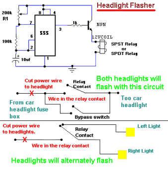
Headlight Flasher
A compact and intriguing circuit designed to flash automotive headlights. It utilizes a well-known NE555 timer circuit to achieve this functionality.
The circuit operates by employing the NE555 timer in astable mode, which allows it to generate a continuous square wave...
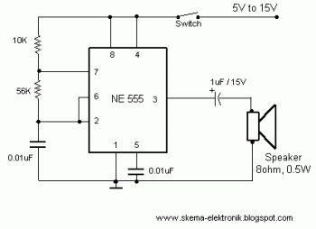
Electronic Buzzer with IC timer NE555 circuit diagram
This easy electronic buzzer circuit is built based on a timer that operates to generate frequency. The IC timer NE555 is used as an astable multivibrator operating at approximately 1 kHz, producing a sound when powered on. The sound frequency...
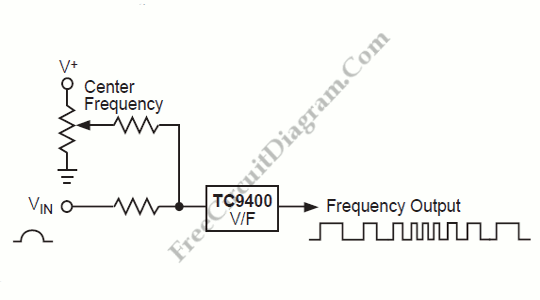
Superlinear FM (Frequency Modulator)
Designing various electronic circuit systems (synthesizer, modem, decoder, data converter, etc.) often requires a frequency modulator subsystem. An FM modulator is a crucial component in these systems.
An FM modulator is an electronic device that encodes information in a carrier wave...
TWO OUADRANT EXPONENTIAL CONTROL
This circuit utilizes a dual operational amplifier (TL082) to create a voltage-controlled oscillator (VCO). The specified component values allow the output frequency to range from 100 Hz to 10 kHz when the input control voltage is between 0.05 and 10...
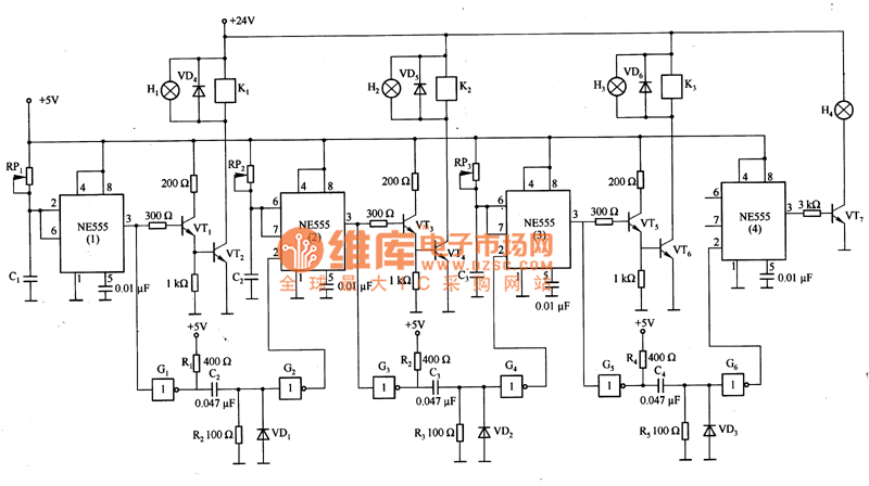
Sequence timer diagram composed by NE555
This is a sequence timer diagram composed of an NE555 timer. The timer can be set to any duration when the power is connected, allowing it to control an external system. In the circuit, K1-K3 are relays used to activate...
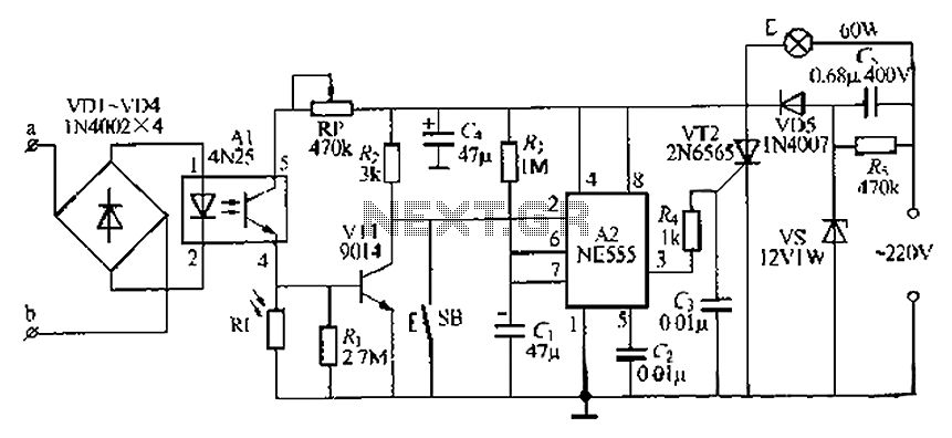
Telephone control automatic lamp circuit 2
The lamp base circuit integrates an NE555 timer and optocouplers to automatically activate the light when a phone call is received at night. The lamp will self-extinguish after a delay. Additionally, a switch allows manual control of the lamp. The...
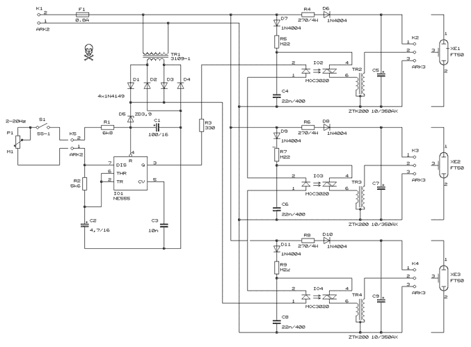
Triple Stroboscope
This circuit allows for the observation of movement between various stroboscopes. The generation of a rectangular signal is accomplished using an NE555 timer IC. The circuit operates on a low power supply, which is created using a simple transformer (TR1),...
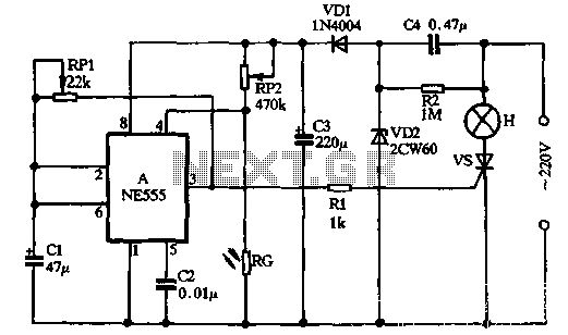
Flashing warning light produced by light control NE555 circuit
VDI, VD2, C3, and C4 form a simple half-wave rectifier capacitor step-down regulator circuit. This circuit can output approximately 12V DC voltage after power is applied across C3, which is utilized for the time base circuit. Additionally, the time base...
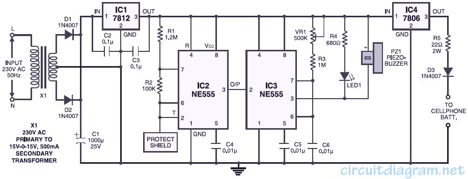
Cell Phone Shield with Charger
The cell phone shield circuit employs two NE555 timer integrated circuits (ICs): one configured as a simple astable multivibrator (IC2) and the second as a monostable multivibrator (IC3). The astable multivibrator utilizes timing resistors R1 and R2 but does not...