


For driving the power supply circuit of the sensor bridge
#OP amplifier
#Zener diode
#voltage reference
#sensor bridge
#10V input
#stability
#circuit design
#analog electronics
#voltage regulation
#precision
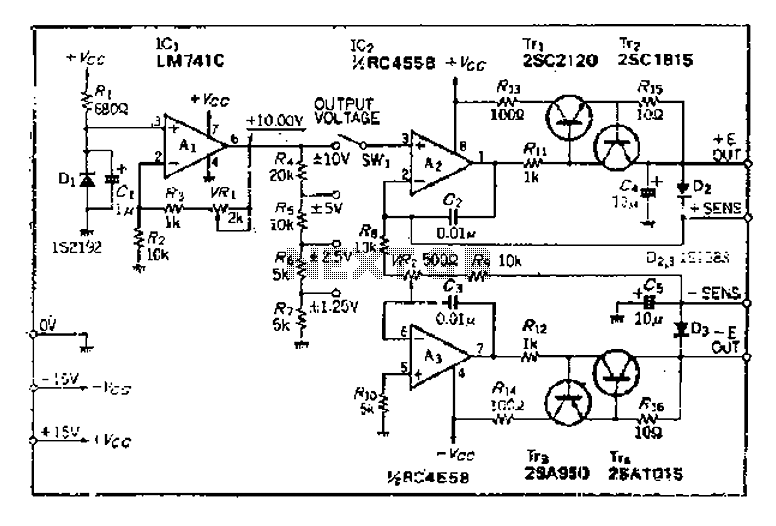
Description: The maximum input voltage is 10V. An operational amplifier (op-amp) is used to provide a reference voltage of 10V, with its stability primarily determined by the characteristics of a temperature-compensated Zener diode (IS2192). The Zener voltage (Vz) can be adjusted using a variable resistor to minimize error. A resistor divider circuit (R4/R1) is employed to switch the input voltage of the op-amp, allowing for a descending order of voltage levels. For maintaining voltage accuracy over time, the resistance must be selected with minimal variation, ideally between 0.5 to 10 ohms. An op-amp buffer amplifier is utilized, with a gain of 1, which is configured positively. Additionally, an inverting amplifier configuration is implemented to convert the output voltage into a negative voltage. Corrections for resistance errors are made using a variable resistor, enabling the achievement of precise voltage output.
The circuit design features a maximum input voltage specification of 10V, which is critical for ensuring the safety and functionality of the operational amplifier (op-amp) employed in the circuit. The reference voltage of 10V is generated through the op-amp, which operates in conjunction with a temperature-compensated Zener diode (IS2192). The Zener diode is selected for its stability across varying temperatures, which is essential for maintaining a consistent output voltage.
The Zener voltage (Vz) can be fine-tuned via a variable resistor, allowing for precise adjustments to counteract any discrepancies that may arise during operation. This variable resistor is crucial for calibrating the circuit to achieve the desired performance specifications. A resistor divider circuit, consisting of resistors R4 and R1, is implemented to facilitate the switching of input voltage levels to the op-amp. This configuration is designed to provide a descending order of input voltages, which can be beneficial for applications requiring varying voltage levels.
To ensure sustained voltage accuracy over time, it is imperative to select resistances that exhibit minimal variation. The recommended range for these resistances is between 0.5 to 10 ohms, which helps to mitigate the effects of drift and enhances the reliability of the circuit.
The circuit incorporates an op-amp buffer amplifier with a gain of 1, which serves to isolate the input from the output, thereby preventing loading effects that could compromise performance. The buffer amplifier is configured positively, ensuring that the output voltage remains in phase with the input voltage. Furthermore, an inverting amplifier configuration is employed to produce a negative voltage output from the circuit. This is achieved by utilizing feedback through a resistor network, which allows for the inversion of the output voltage while maintaining accuracy.
To address potential resistance errors, a variable resistor is included in the design. This component allows for real-time adjustments, facilitating the correction of any inaccuracies in the voltage output. The implementation of these design elements collectively ensures that the circuit operates efficiently, providing stable and precise voltage references as required for various electronic applications.A. The maximum input voltage of 10V. OP amplifier A, to give ten of 10V reference voltage, and its stability is mainly determined by the Zener diode characteristics, mining com mission temperature compensated zener diode (IS2192). Zener voltage Vz if the error can be used to adjust the variable resistor, it is IO. oov. s resistor divider circuit (R4vR,) to switch A, input voltage, ul/2 office units in descending order. When you need to 1 voltage accuracy over time, EU resistance must choose a small difference in disrespect of the product ( 0.5 ~ .10 {).
OP/Ze buffer amplifier 4. The amplifier, save magnification is 1, is positive to put large, but with sleep} line inverting amplifier, the output voltage into a negative voltage inverter output voltage. - said that the resistance r, four errors on a variable resistor r z mouth into line correction, accurate voltage can be obtained.
The circuit design features a maximum input voltage specification of 10V, which is critical for ensuring the safety and functionality of the operational amplifier (op-amp) employed in the circuit. The reference voltage of 10V is generated through the op-amp, which operates in conjunction with a temperature-compensated Zener diode (IS2192). The Zener diode is selected for its stability across varying temperatures, which is essential for maintaining a consistent output voltage.
The Zener voltage (Vz) can be fine-tuned via a variable resistor, allowing for precise adjustments to counteract any discrepancies that may arise during operation. This variable resistor is crucial for calibrating the circuit to achieve the desired performance specifications. A resistor divider circuit, consisting of resistors R4 and R1, is implemented to facilitate the switching of input voltage levels to the op-amp. This configuration is designed to provide a descending order of input voltages, which can be beneficial for applications requiring varying voltage levels.
To ensure sustained voltage accuracy over time, it is imperative to select resistances that exhibit minimal variation. The recommended range for these resistances is between 0.5 to 10 ohms, which helps to mitigate the effects of drift and enhances the reliability of the circuit.
The circuit incorporates an op-amp buffer amplifier with a gain of 1, which serves to isolate the input from the output, thereby preventing loading effects that could compromise performance. The buffer amplifier is configured positively, ensuring that the output voltage remains in phase with the input voltage. Furthermore, an inverting amplifier configuration is employed to produce a negative voltage output from the circuit. This is achieved by utilizing feedback through a resistor network, which allows for the inversion of the output voltage while maintaining accuracy.
To address potential resistance errors, a variable resistor is included in the design. This component allows for real-time adjustments, facilitating the correction of any inaccuracies in the voltage output. The implementation of these design elements collectively ensures that the circuit operates efficiently, providing stable and precise voltage references as required for various electronic applications.A. The maximum input voltage of 10V. OP amplifier A, to give ten of 10V reference voltage, and its stability is mainly determined by the Zener diode characteristics, mining com mission temperature compensated zener diode (IS2192). Zener voltage Vz if the error can be used to adjust the variable resistor, it is IO. oov. s resistor divider circuit (R4vR,) to switch A, input voltage, ul/2 office units in descending order. When you need to 1 voltage accuracy over time, EU resistance must choose a small difference in disrespect of the product ( 0.5 ~ .10 {).
OP/Ze buffer amplifier 4. The amplifier, save magnification is 1, is positive to put large, but with sleep} line inverting amplifier, the output voltage into a negative voltage inverter output voltage. - said that the resistance r, four errors on a variable resistor r z mouth into line correction, accurate voltage can be obtained.
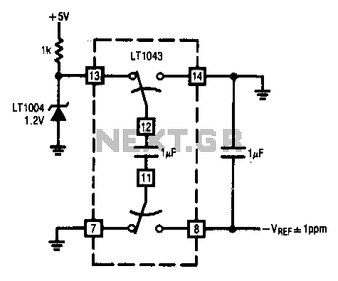
Precision-voltage-inverter
This circuit enables the inversion of a reference signal with an accuracy of 1 ppm. It features high input impedance and does not require any trimming.
The described circuit is designed to invert a reference voltage signal while maintaining a high...
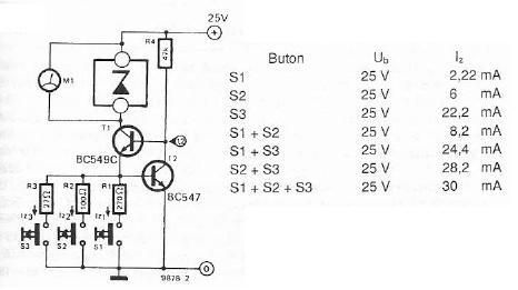
zener diode tester schematic
The electronic scheme provided can be used to design a Zener diode tester utilizing a few electronic components. This Zener tester, in conjunction with a multimeter, allows for the precise measurement of the threshold voltage of a Zener diode. The...
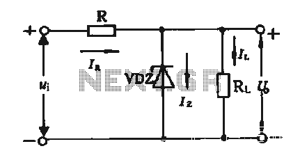
Regulator circuit silicon resistor formed
The simple voltage regulator circuit consists of a silicon regulator and a resistor. It is designed to rectify and filter DC voltage, as illustrated in the accompanying figure. The voltage regulator is connected in parallel with the load, and the...
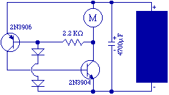
Zener-based solar engine
The capacitor charges until the PNP transistor (here shown as a 2N3906, but you could also use a BC327) receives base current through the Zener and turns on. Then the NPN transistor (here shown as a 2N3904, but you could...
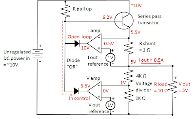
how does power supply regulate its
Most power supplies regulate either their output voltage or current at a constant level, depending on the load resistance relative to the power supply's output voltage and current settings. This can be summarized as follows: To accomplish this, most power...
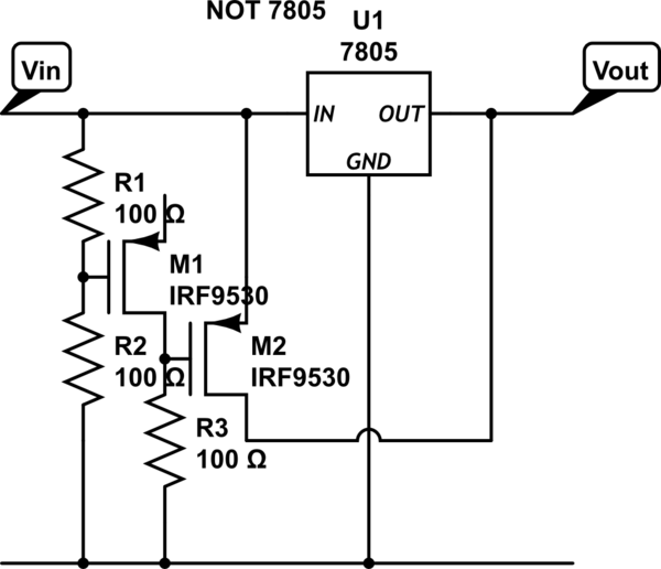
power Voltage supply clipping to <=3.3V
Supply it with a Li-Ion cell, which has a voltage range of 2.7 to 4.2V. The complexity of a buck/boost converter is not desired. While it is possible to regulate the voltage down to anything below 2.5V, it would be...

capacitor Explaining a car voltage regulator circuit
The circuit regulates approximately 12V from the car battery down to 5V for use by an Atmel AVR microcontroller. The presence of two capacitors on each side of the linear regulator LM7805 raises questions regarding their purpose. It is suggested...
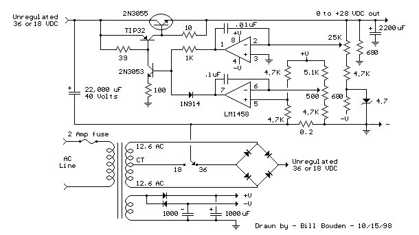
Current and Variable Voltage Power Supply
Another adjustment of application operational amplifiers to adapt a power supply is apparent below. The power supply requires an additional adjustment to supply the op-amps with a bipolar voltage (+/- 8 volts), and the negative voltage is also used to...
Regulator circuit silicon resistor formed
The simple voltage regulator circuit consists of a silicon regulator and a resistor. It is designed to rectify and filter DC voltage, as illustrated in the accompanying figure. The voltage regulator is connected in parallel with the load, and the...