


1880MHz internal bias circuit diagram of the amplifier application collector RF2324
#RF2324
#amplifier
#1880MHz
#bias circuit
#preamplifier
#RF signal
#collector
#radio frequency
#circuit diagram
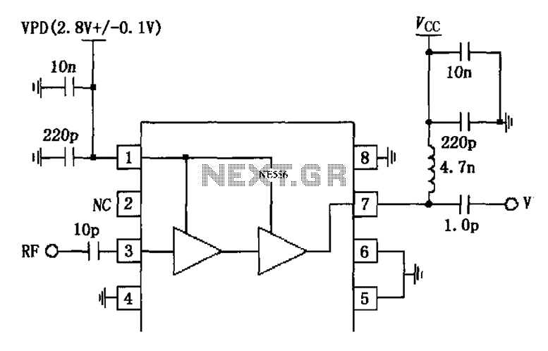
Description: The circuit is constituted by the RF2324 1880MHz internal amplifier collector bias application. A radio frequency (RF) signal enters through input pin 3 and is processed by a preamplifier. The final stage power amplifier output is amplified by 7 feet. The output is directly coupled to the internal amplifier through a 10pF capacitance, which serves to block DC while providing impedance matching at 1880MHz to 50 ohms. The 7 feet open collector output terminal can be connected to the power supply (Vcc) via a choke or matching inductor, where the pin impedance matching is typically 50 ohms. An external output matching network is utilized to ensure the amplifier output impedance is matched for maximum output power and efficiency. The 1 foot pin functions as a power-down control terminal. When VPD is at 2.8V ± 0.1V (with IPD typically at 8.5mA), the circuit is active; when VPD is at 0.9V, the circuit shuts down. An additional RF bypass circuit is required for VPD.
The RF2324 amplifier circuit operates at a frequency of 1880MHz, primarily used in wireless communication applications. The RF signal enters through pin 3, where it is initially amplified by a preamplifier stage. This preamplification is crucial for enhancing the weak RF signals to a level suitable for further processing. The term "7 feet" refers to the distance or the layout of the circuit traces, which can influence the signal integrity and performance due to parasitic capacitance and inductance.
The internal amplifier is coupled with a 10pF capacitor, which is strategically placed to block any DC components while allowing the RF signal to pass through. This coupling capacitor is essential in maintaining the desired signal characteristics while preventing DC bias from affecting the amplifier's operation. Impedance matching at 50 ohms is critical in RF circuits to minimize signal reflections and maximize power transfer, which is achieved through careful design of the external output matching network.
The open collector output terminal, referred to as "7 feet," can connect to a power supply (Vcc) through either a choke or a matching inductor. This connection aids in stabilizing the voltage supply and filtering out unwanted noise. The external output matching network is designed to ensure that the amplifier's output impedance aligns with the system's requirements, optimizing both output power and efficiency.
The power-down control terminal, indicated as "1 foot," allows for the circuit to be turned off when not in use, thereby conserving power. The specified voltage levels for VPD are critical for the operation of the circuit; a voltage of 2.8V ± 0.1V keeps the circuit active, while a drop to 0.9V effectively disables it. The need for an additional RF bypass circuit for VPD indicates that further filtering may be necessary to ensure stable operation and prevent unwanted oscillations or noise from affecting the amplifier's performance. Overall, this circuit design exemplifies careful consideration of RF principles to achieve reliable and efficient amplification in communication systems. As shown in FIG constituted by RF2324 1880MHz internal amplifier collector bias application circuit. Radio frequency (RF) signal from the input pin 3, via a preamplifier, after the last stage power amplifier output is amplified by 7 feet. 3 feet directly coupled to the internal amplifier, thus blocking plus a 10pF of capacitance coupling, impedance matching at 1880MHz work to 50. 7 feet for the open collector output terminal can be connected to the power supply Vcc through choke or matching inductor, the pin impedance matching is typically 50, external output matching network allows the amplifier output impedance matching for maximum output power and efficiency.
1 foot for the power down control terminal. When VPD 2.8V 0.1V when (IPD is typically 8.5mA) circuit; when VPD 0.9V circuit closes. VPD requested additional RF bypass circuit.
The RF2324 amplifier circuit operates at a frequency of 1880MHz, primarily used in wireless communication applications. The RF signal enters through pin 3, where it is initially amplified by a preamplifier stage. This preamplification is crucial for enhancing the weak RF signals to a level suitable for further processing. The term "7 feet" refers to the distance or the layout of the circuit traces, which can influence the signal integrity and performance due to parasitic capacitance and inductance.
The internal amplifier is coupled with a 10pF capacitor, which is strategically placed to block any DC components while allowing the RF signal to pass through. This coupling capacitor is essential in maintaining the desired signal characteristics while preventing DC bias from affecting the amplifier's operation. Impedance matching at 50 ohms is critical in RF circuits to minimize signal reflections and maximize power transfer, which is achieved through careful design of the external output matching network.
The open collector output terminal, referred to as "7 feet," can connect to a power supply (Vcc) through either a choke or a matching inductor. This connection aids in stabilizing the voltage supply and filtering out unwanted noise. The external output matching network is designed to ensure that the amplifier's output impedance aligns with the system's requirements, optimizing both output power and efficiency.
The power-down control terminal, indicated as "1 foot," allows for the circuit to be turned off when not in use, thereby conserving power. The specified voltage levels for VPD are critical for the operation of the circuit; a voltage of 2.8V ± 0.1V keeps the circuit active, while a drop to 0.9V effectively disables it. The need for an additional RF bypass circuit for VPD indicates that further filtering may be necessary to ensure stable operation and prevent unwanted oscillations or noise from affecting the amplifier's performance. Overall, this circuit design exemplifies careful consideration of RF principles to achieve reliable and efficient amplification in communication systems. As shown in FIG constituted by RF2324 1880MHz internal amplifier collector bias application circuit. Radio frequency (RF) signal from the input pin 3, via a preamplifier, after the last stage power amplifier output is amplified by 7 feet. 3 feet directly coupled to the internal amplifier, thus blocking plus a 10pF of capacitance coupling, impedance matching at 1880MHz work to 50. 7 feet for the open collector output terminal can be connected to the power supply Vcc through choke or matching inductor, the pin impedance matching is typically 50, external output matching network allows the amplifier output impedance matching for maximum output power and efficiency.
1 foot for the power down control terminal. When VPD 2.8V 0.1V when (IPD is typically 8.5mA) circuit; when VPD 0.9V circuit closes. VPD requested additional RF bypass circuit.
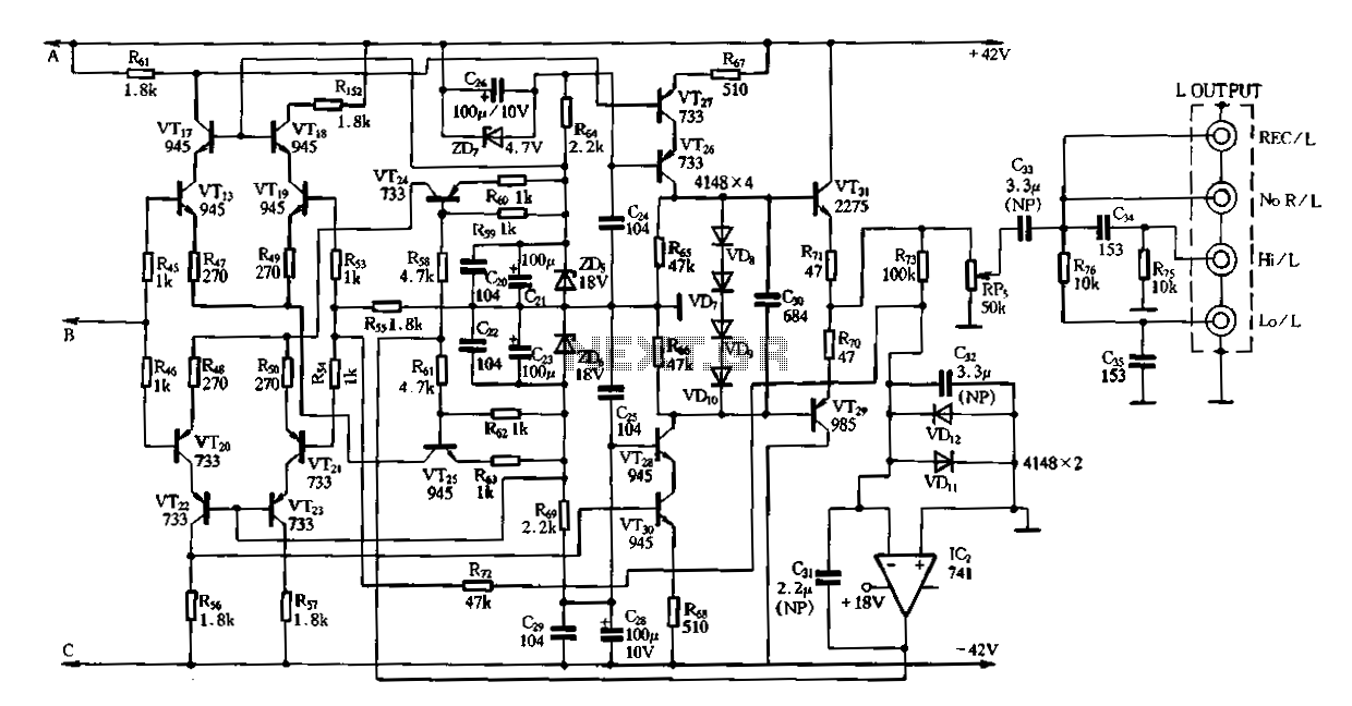
Vanda F-9500A preamplifier b
Figure 3-2 (b) represents the second half of the circuit, where transistors VT17 to VT31 are configured as power amplifiers and pre-amplifiers. This section is structurally identical to the operational integrated circuit IC2 and includes zero servos. The circuit is...
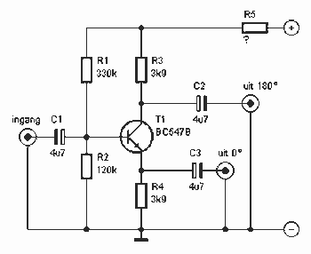
Amplifiers connecting Bridge
This is a circuit that ensures that you can connect two amplifiers together so you get more power. When called in bridge linking two amplifiers plus you can link the outputs of the amplifiers to the speaker. One of the...
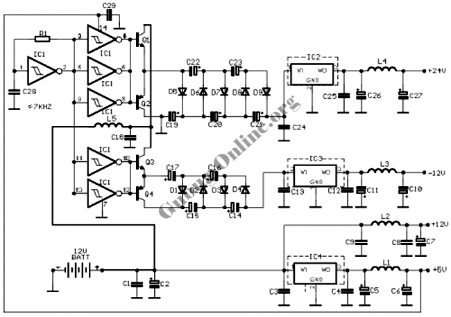
DC-Coupled Audio Amplifier Circuit
This design circuit for audio amplifiers with DC coupling to the load is not commonly used today, despite its clear advantages. One advantage is the elimination of the need for a second (symmetric) power supply, and another is the improved...
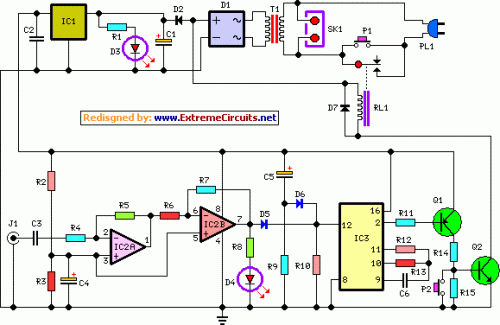
Amplifier Timer Circuit Schematic
This circuit turns off an amplifier or any other device when a low-level audio signal fed to its input is absent for at least 15 minutes. Pressing P1 switches the device on, supplying power to any appliance connected to SK1....
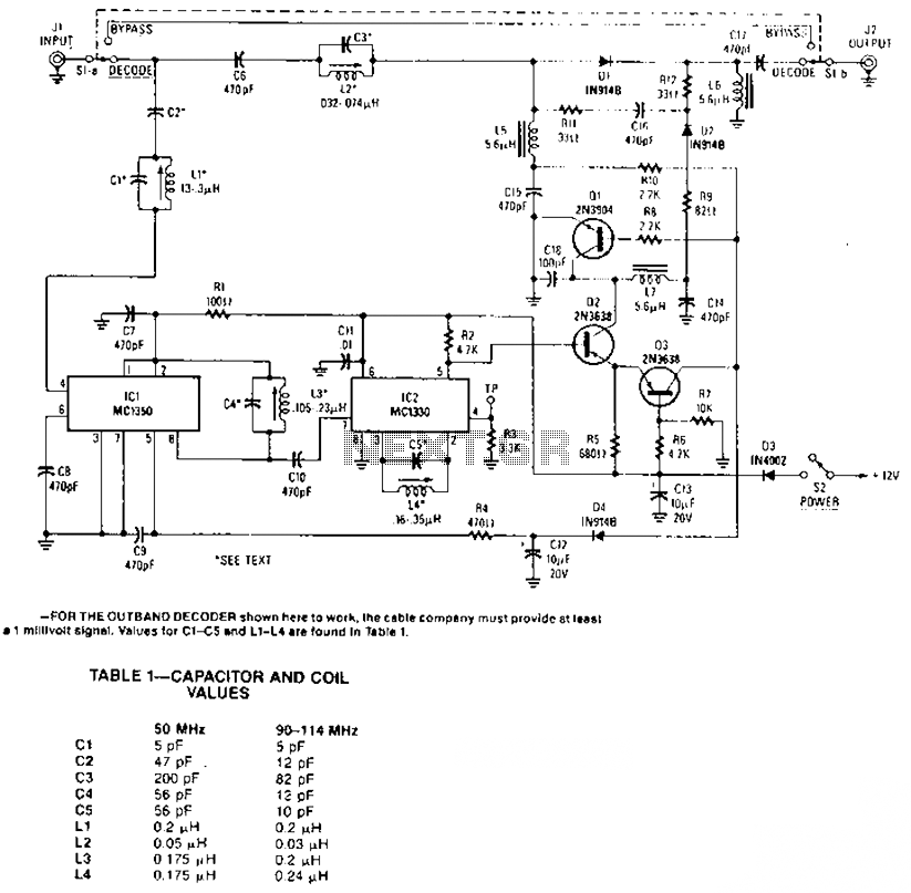
Band decoder circuit diagram
The circuit amplifier and attenuator control video detector consists of a composition for the synchronization channel. The synchronization interval is where the gain circuit is increased.
The described circuit involves an amplifier and an attenuator that work together to control a...
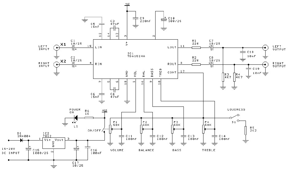
Preamplifier + tone control circuit based TDA1524A
Preamplifier and tone control circuit based on the TDA1524A. The tone control circuit module is included in this preamplifier circuit, allowing for direct connection of the output channels to a stereo power audio amplifier circuit. This RIAA stereo preamplifier utilizes...
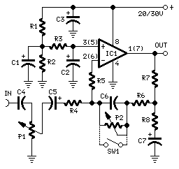
Stereo Preamplifier with Bass-boost
The preamplifier in question is engineered to interface with various audio devices such as CD players, tuners, and tape recorders. Its primary function is to provide an alternating current (AC) voltage gain of 4, an attribute that allows it to...
RECEIVER BUILDING BLOCKS
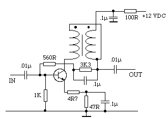
This amplifier has about 20dB of gain, bandwidth of 100MHz and noise figure of about 7dB. The output transformer is 8 turns bifilar wound on a ferrite core. Use a medium power UHF transistor 2N5109, 2N3866, 2N4427 or similar. The...
Stabilized-amplifier
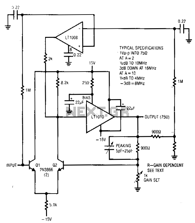
This amplifier operates across a broad range of gains, typically from 1 to 10. It integrates the LT1010 with a fast discrete stage and an LT1008-based destabilizing loop. Transistors Q1 and Q2 create a differential stage that converts to a...