


830MHz RF2104 power amplifier schematic circuit configuration
#RF2104
#830MHz
#power amplifier
#preamplifier
#amplifier stage
#RF signal
#schematic
#circuit configuration
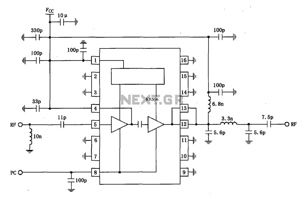
Description: The RF2104 830MHz amplifier circuit operates as illustrated in the figure. A radio frequency (RF) signal enters through a 5-foot input, passes through a preamplifier, and is then amplified by an amplifier stage at the 12-pin output. The circuit includes a 5-foot DC voltage line, a 5-foot line with a DC blocking capacitor for coupling, and a shunt inductor (10nH) in parallel. The input impedance is 50 ohms. Pins 12 and 13 are connected internally within the chip, with pins 13 and 14 typically connected externally for signal output. An output matching network is employed to ensure that the amplifier's output impedance matches the load impedance of pin 5 + j0 to achieve maximum output power. Pins 13 and 14 are also connected to an external power supply, serving as the final stage amplifier output. Pin 8 serves as the power control pin (PC), which can be connected to 0V or 3V to control the gain. If gain control is not necessary, this pin may be fixed at a voltage between 2.5V and 3V, with a maximum current inflow of 1mA.
The RF2104 amplifier circuit is designed for high-frequency applications, operating at 830MHz, making it suitable for various RF communication systems. The preamplifier stage is crucial for boosting weak RF signals before they reach the main amplification stage, ensuring that the subsequent amplification is effective and maintains signal integrity.
The output section of the circuit is carefully designed to provide an optimal impedance match between the amplifier and the load. The output matching network plays a vital role in maximizing power transfer and minimizing signal reflections, which could otherwise degrade performance. The choice of a 10nH shunt inductor aids in tuning the output stage to achieve the desired impedance characteristics.
The gain control feature via pin 8 allows for flexibility in the amplifier's performance, enabling users to adjust the amplification level based on the application requirements. This control can be particularly useful in environments where signal conditions fluctuate, allowing the amplifier to adapt and maintain optimal performance.
Overall, the RF2104 amplifier circuit exemplifies a well-engineered solution for enhancing RF signals, with features that cater to both performance and adaptability in various electronic applications. As shown in FIG constituted by RF2104 830MHz *** amplifier circuit works. Radio frequency (RF) signal from 5 feet input, via a preamplifier, amplified by an amplifier stage aft er the end of the 12-pin output. 5 feet with DC voltage, 5 feet plus a DC blocking capacitor coupling, while in parallel with a shunt inductor (10nH), 5 feet input impedance of 50. 12,13 pin output terminal is connected inside the chip, usually 13-14 feet connected together externally as a signal output, the output matching network connected, the amplifier output impedance to match the impedance of the load pin 5 + j0 when available obtain maximum output power.
13-14 feet is also connected with an external power supply as the end of the final stage amplifier. 8 feet to power control pin (PC), you can control the pin is connected to 0V and 3V gain, thereby controlling power; when the gain control is not required, the foot may be connected to a fixed voltage of 2.5 ~ 3V; the feet to the inflow of 2.5V voltage pin maximum current 1mA.
The RF2104 amplifier circuit is designed for high-frequency applications, operating at 830MHz, making it suitable for various RF communication systems. The preamplifier stage is crucial for boosting weak RF signals before they reach the main amplification stage, ensuring that the subsequent amplification is effective and maintains signal integrity.
The output section of the circuit is carefully designed to provide an optimal impedance match between the amplifier and the load. The output matching network plays a vital role in maximizing power transfer and minimizing signal reflections, which could otherwise degrade performance. The choice of a 10nH shunt inductor aids in tuning the output stage to achieve the desired impedance characteristics.
The gain control feature via pin 8 allows for flexibility in the amplifier's performance, enabling users to adjust the amplification level based on the application requirements. This control can be particularly useful in environments where signal conditions fluctuate, allowing the amplifier to adapt and maintain optimal performance.
Overall, the RF2104 amplifier circuit exemplifies a well-engineered solution for enhancing RF signals, with features that cater to both performance and adaptability in various electronic applications. As shown in FIG constituted by RF2104 830MHz *** amplifier circuit works. Radio frequency (RF) signal from 5 feet input, via a preamplifier, amplified by an amplifier stage aft er the end of the 12-pin output. 5 feet with DC voltage, 5 feet plus a DC blocking capacitor coupling, while in parallel with a shunt inductor (10nH), 5 feet input impedance of 50. 12,13 pin output terminal is connected inside the chip, usually 13-14 feet connected together externally as a signal output, the output matching network connected, the amplifier output impedance to match the impedance of the load pin 5 + j0 when available obtain maximum output power.
13-14 feet is also connected with an external power supply as the end of the final stage amplifier. 8 feet to power control pin (PC), you can control the pin is connected to 0V and 3V gain, thereby controlling power; when the gain control is not required, the foot may be connected to a fixed voltage of 2.5 ~ 3V; the feet to the inflow of 2.5V voltage pin maximum current 1mA.
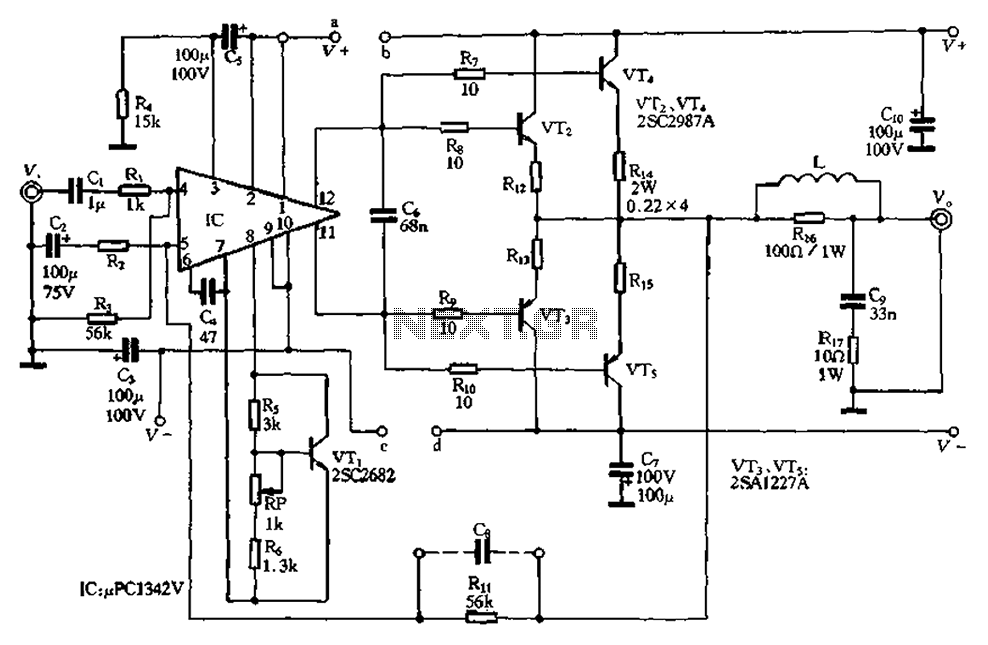
Compact 100W power amplifier circuit
The pLPC1342V and NE are two companies involved in a tube amplifier circuit utilizing 2SA1227A and 2SC2987A transistors, achieving a maximum output power of up to 120W with a cutoff frequency of up to 500 MHz. The circuit, illustrated in...
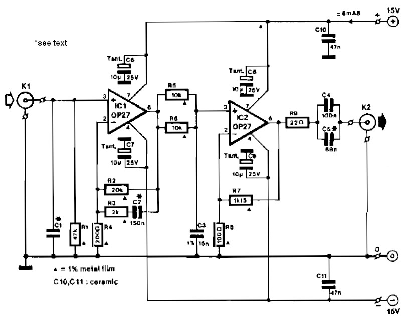
Preamplifier for magnetic phono cartridges schematics
Circuit IC1 provides a gain amplification of 40 dB, which decreases to approximately 20 dB when the frequency exceeds 500 Hz. To reduce resistor noise and the load on the operational amplifier at higher frequencies, the value of resistor R3...
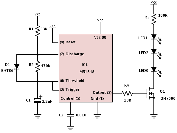
Building a device from a schematic
A common issue encountered is that individuals possess a schematic, also known as a circuit diagram, that they wish to construct. However, they discover that there are...
Building a circuit from a schematic requires a clear understanding of the components involved...
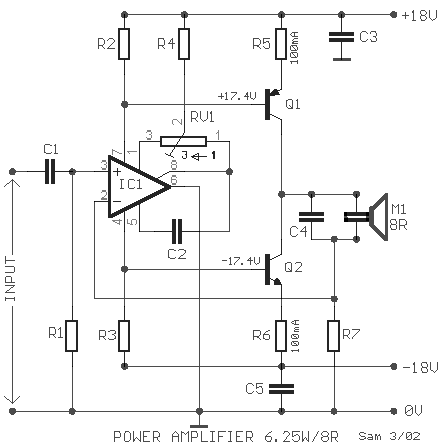
Power amplifier for Loudspeaker 6.5W 8R circuit
The amplifier circuit utilizes negative current feedback, which ensures that the load current is primarily influenced by the input signal rather than the loudspeaker's impedance. The inductor current from the loudspeaker generates a voltage across resistor R7, which is fed...
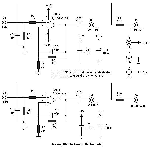
50 Watt power Amplifier with preamplifier and headphone output
The amplifier drives a pair of loudspeakers using two LM3876 integrated power amp ICs (50 watts per channel), or a pair of headphones via a Meier crossfeed filter and an OPA2134 dual opamp. It provides four switchable line level inputs,...
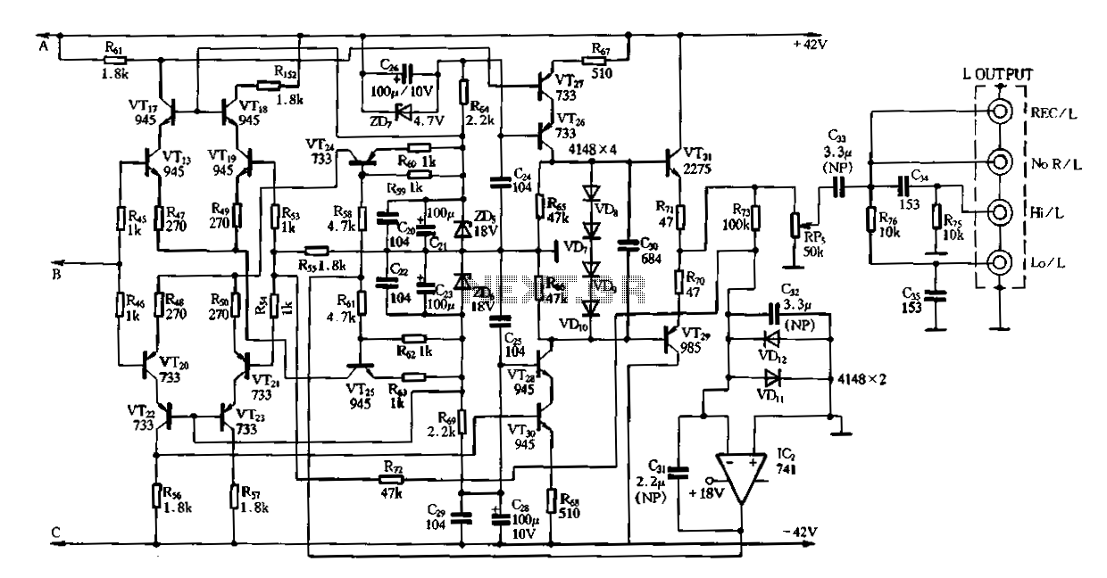
Vanda F-9500A preamplifier b
Figure 3-2 (b) represents the second half of the circuit, where transistors VT17 to VT31 are configured as power amplifiers and pre-amplifiers. This section is structurally identical to the operational integrated circuit IC2 and includes zero servos. The circuit is...
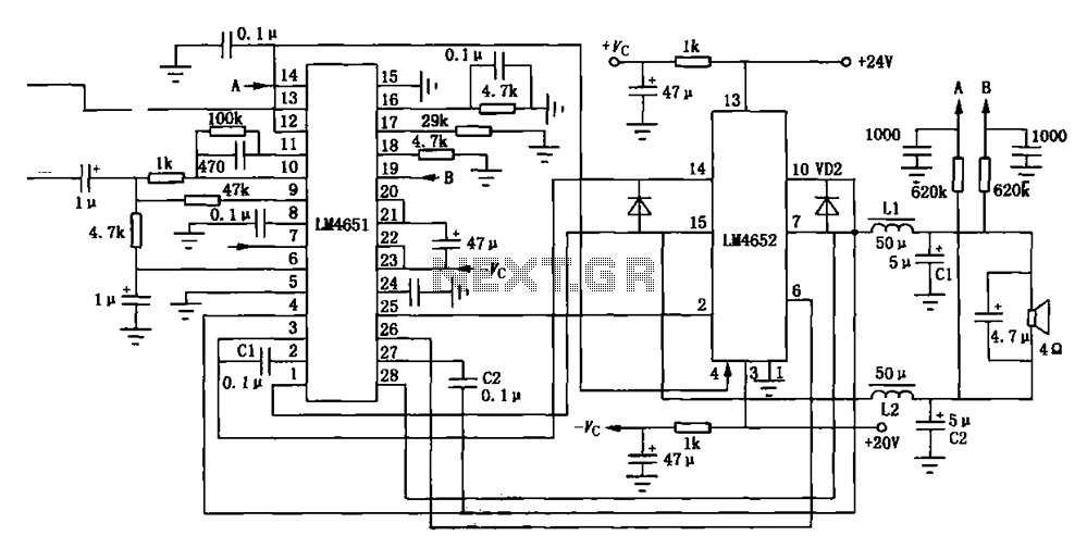
LM4561 LM4562 consisting of 170W power amplifier circuit
Figure (a) illustrates a 170W output amplifier circuit designed for a 4-ohm load. The LM4651 is a class D amplifier presented in a 28-pin DIP package, with its internal equivalent circuit depicted in Figure (c).
The 170W output amplifier circuit is...
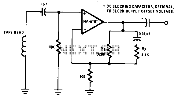
Playback-preamplifier
The preamplifier is designed to offer a low-frequency boost at 50 Hz, maintain a flat response up to 3 kHz, and attenuate high frequencies above 3 kHz. Compensation for variations in tape and tape head performance can be accomplished by...
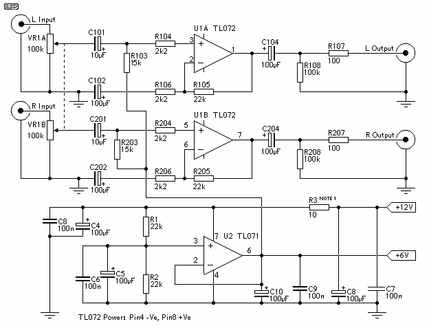
Simple Car Preamplifier and Artificial Earth
The preamp circuit is completely conventional, and by necessity is AC coupled throughout. The artificial earth is derived by two resistors (R1 and R2), which will set the "earth" at exactly 1/2 the supply voltage. This is nominally 13.8V in...