


Azures Realm
#frequency-hopping
#microwave
#signal generator
#continuous wave
#FCC compliant
#FR4
#Part 15
#RF
#wireless
#communication

Description: The primary project involved designing a frequency-hopping microwave signal generator. The device was required to transmit a continuous wave (CW) signal at a specific frequency and then switch to subsequent frequencies. Compliance with Part 15 FCC regulations was necessary. The board was to be manufactured using FR4 and copper on the school’s milling machine. A voltage-controlled oscillator (VCO) was responsible for generating the carrier wave, controlled through a feedback loop utilizing a phase-locked loop (PLL) chip. The PLL's frequency set-point is programmable via an SPI connection with a PIC microcontroller, which facilitates the frequency-hopping feature. A crystal oscillator provides a 10 MHz reference signal for the PLL. The VCO output is filtered through a band-pass filter to eliminate out-of-band components, followed by an RF amplifier to increase the signal to the required output power of 7 dBm. All components were specified by the instructor, except for the microcontroller. Although a custom MSP430 microcontroller board was recommended, the decision was made to use the PIC due to greater familiarity. In the design of the PLL, the loop filter is a critical component. Two key parameters influencing loop filter design are loop bandwidth and phase margin. The loop bandwidth affects the lock time, with a maximum lock time requirement of 0.4 seconds. Typically, a transmitter would utilize most of this duration to transmit data. The PLL was designed to achieve a lock time within 100 microseconds, leading to a loop bandwidth setting of 50 kHz. Simulations indicated a lock time of only 40 microseconds, satisfying the requirements. Calculations and simulations were conducted using ADIsimPLL. Feedback from the VCO is essential for frequency matching, necessitating a split of the VCO output. A Wilkinson divider was employed for this purpose, offering advantages such as being lossless in the forward direction, inherent matching at all ports (assuming equal power split), and good isolation between output ports. The typical layout for a 3 dB Wilkinson divider is depicted in Figure 5. The divider was designed and optimized using ADS to achieve S(2, 1) and S(3, 1) values as close to 3 dB as possible at 5.8 GHz, matched to 50 ohms. An equal power split was chosen for simplicity, as no specific need for an uneven split was identified. One output leg of the divider connects to the band-pass filter and RF amplifier leading to the circuit output, while the other leg feeds back to the PLL reference input. The divider was simulated in Momentum, providing approximately -3.4 dB at both output ports across the 5.725-5.850 GHz frequency range. The band-pass filter was designed to center around 5.7875 GHz with a flat response over a bandwidth of 125 MHz. A coupled line design with a maximally-flat response was utilized to facilitate fabrication and ensure a flat response across the desired frequency range. A low-order (N=2) filter was selected, as higher-order designs proved to be excessively lossy. The simulated response demonstrated a flat passband within the frequency range of interest, with an attenuation of about -4 dB, which would be compensated by the subsequent amplifier. The design incorporated a Microchip PIC184F2321 28-pin microcontroller to manage the PLL and implement frequency hopping. This microcontroller was chosen for its availability and ease of programming. The PIC was integrated onto the same board and communicates with the PLL via an SPI interface, configuring the frequency of operation by loading a series of 24-bit latches. With the correct latch configuration, the PLL selects the voltage for the VCO and locks onto the desired frequency. The PIC was programmed with a list of 75 different frequencies for the hopping sequence.
The frequency-hopping microwave signal generator is a sophisticated electronic device that leverages several key components to achieve its operational goals. The VCO serves as the heart of the system, generating a continuous wave signal that is modulated in frequency through the PLL. The PLL is crucial for maintaining the stability and accuracy of the frequency output, ensuring that the VCO locks onto the desired frequency swiftly, as dictated by the loop bandwidth and phase margin parameters.
The Wilkinson divider plays a vital role in the feedback mechanism, allowing for effective power distribution to both the output stage and the PLL. Its design ensures minimal signal loss and optimal performance across the specified frequency range, which is essential for maintaining signal integrity in microwave applications. The band-pass filter further refines the output, ensuring that only the desired frequency components are transmitted while suppressing unwanted signals.
The choice of microcontroller is significant in this design, as it not only facilitates the control of the PLL but also manages the frequency hopping sequence. The use of SPI for communication between the microcontroller and PLL allows for rapid configuration changes, enabling the generator to switch frequencies efficiently.
Overall, the project exemplifies a comprehensive approach to designing a frequency-hopping microwave signal generator, integrating various electronic components and design principles to meet specific regulatory and performance requirements. The careful selection of each element, from the VCO to the microcontroller, underscores the importance of precision and reliability in microwave signal generation.The main project was to design a frequency-hopping microwave signal generator. Although the device wouldn`t actually modulate any data, it would have to send a continuous wave (CW) signal on a frequency, then hop to the next frequency. The device had to be Part 15 FCC compliant. The device also had to be milled on our school`s machine, which meant the board would be made of FR4
and copper. The carrier wave will be generated by a voltage-controlled oscillator (VCO), which is controlled via a feedback loop with a phase-locked loop (PLL) chip. The frequency set-point of the PLL is programmable via SPI connection with a PIC microcontroller, which will provide the frequency-hopping functionality.
A crystal oscillator provides a 10 MHz reference signal for the PLL. Finally, the VCO output will be filtered through a band-pass filter to remove any out-of-band components, and an RF amplifier will boost the signal to the desired 7dBm output power. All parts were specified by the instructor, except for the microcontroller. A custom MSP430 microcontrolle board was specified, but we decided to use the PIC since I had more experience with it.
In PLL design, the critical component to design is the loop filter. There are two key parameters of the PLL that would have an impact on loop filter design: loop bandwidth and phase margin. The loop bandwidth influences the lock time. In the project requirements, the maximum lock time is 0. 4s. This is a very long time, and normally a transmitter would use most of this time to actually send data.
The PLL should be able to lock within 100us. Based on this requirement, the loop bandwidth is set to 50KHz. The simulation indicated that the lock time is only 40us, which meets our requirement. The calculations and simulations were performed with ADIsimPLL. The PLL requires feedback from the VCO to match frequency, so the VCO output must be split. A Wilkinson divider was used for this purpose, as it provides a number of advantages over other splitting designs: it is (ideally) lossless in the forward direction, it is inherently matched at all ports (assuming an equal power split), and there is good isolation between the two output ports. Figure 5 shows the typical layout for a 3 dB Wilkinson divider. The divider was designed and tuned in ADS to obtain an S(2, 1) and S(3, 1) as close to 3 dB as possible at 5.
8 GHz and matched to 50O. An equal power split was used for ease of design, and because we could determine no particular reason to use an uneven split. One output leg of the divider feeds the BPF and RF amplifier leading to the circuit output, while the other leg feeds back to the PLL reference input.
The divider was simulated in Momentum. The divider provides about -3. 4 dB at both output ports over the entire 5. 725-5. 850 GHz frequency range. The band-pass filter was designed to be centered around 5. 7875 GHz with a flat response over 125 MHz of bandwidth. A coupled line design with a maximally-flat response was implemented so as to ensure ease of fabrication and a flat response over the desired frequency range. A low order (N=2) filter was used as higher order designs proved to be very lossy. The simulated response showed a flat passband in the frequency range of interest, with an attenuation of about -4 dB.
This loss will be offset by the following amplifier. A Microchip PIC184F2321 28-pin microcontroller was selected for the design to control the PLL and implement frequency hopping. This device was selected due to its availability and ease of programming. The PIC was out on the same board and communicates with the PLL via an SPI interface and configures the frequency of operation by loading a series of 24 bit latches.
With the correct latch configuration, the PLL will select the voltage for the VCO and lock to the chosen frequency. The PIC was programmed with a list of 75 di
The frequency-hopping microwave signal generator is a sophisticated electronic device that leverages several key components to achieve its operational goals. The VCO serves as the heart of the system, generating a continuous wave signal that is modulated in frequency through the PLL. The PLL is crucial for maintaining the stability and accuracy of the frequency output, ensuring that the VCO locks onto the desired frequency swiftly, as dictated by the loop bandwidth and phase margin parameters.
The Wilkinson divider plays a vital role in the feedback mechanism, allowing for effective power distribution to both the output stage and the PLL. Its design ensures minimal signal loss and optimal performance across the specified frequency range, which is essential for maintaining signal integrity in microwave applications. The band-pass filter further refines the output, ensuring that only the desired frequency components are transmitted while suppressing unwanted signals.
The choice of microcontroller is significant in this design, as it not only facilitates the control of the PLL but also manages the frequency hopping sequence. The use of SPI for communication between the microcontroller and PLL allows for rapid configuration changes, enabling the generator to switch frequencies efficiently.
Overall, the project exemplifies a comprehensive approach to designing a frequency-hopping microwave signal generator, integrating various electronic components and design principles to meet specific regulatory and performance requirements. The careful selection of each element, from the VCO to the microcontroller, underscores the importance of precision and reliability in microwave signal generation.The main project was to design a frequency-hopping microwave signal generator. Although the device wouldn`t actually modulate any data, it would have to send a continuous wave (CW) signal on a frequency, then hop to the next frequency. The device had to be Part 15 FCC compliant. The device also had to be milled on our school`s machine, which meant the board would be made of FR4
and copper. The carrier wave will be generated by a voltage-controlled oscillator (VCO), which is controlled via a feedback loop with a phase-locked loop (PLL) chip. The frequency set-point of the PLL is programmable via SPI connection with a PIC microcontroller, which will provide the frequency-hopping functionality.
A crystal oscillator provides a 10 MHz reference signal for the PLL. Finally, the VCO output will be filtered through a band-pass filter to remove any out-of-band components, and an RF amplifier will boost the signal to the desired 7dBm output power. All parts were specified by the instructor, except for the microcontroller. A custom MSP430 microcontrolle board was specified, but we decided to use the PIC since I had more experience with it.
In PLL design, the critical component to design is the loop filter. There are two key parameters of the PLL that would have an impact on loop filter design: loop bandwidth and phase margin. The loop bandwidth influences the lock time. In the project requirements, the maximum lock time is 0. 4s. This is a very long time, and normally a transmitter would use most of this time to actually send data.
The PLL should be able to lock within 100us. Based on this requirement, the loop bandwidth is set to 50KHz. The simulation indicated that the lock time is only 40us, which meets our requirement. The calculations and simulations were performed with ADIsimPLL. The PLL requires feedback from the VCO to match frequency, so the VCO output must be split. A Wilkinson divider was used for this purpose, as it provides a number of advantages over other splitting designs: it is (ideally) lossless in the forward direction, it is inherently matched at all ports (assuming an equal power split), and there is good isolation between the two output ports. Figure 5 shows the typical layout for a 3 dB Wilkinson divider. The divider was designed and tuned in ADS to obtain an S(2, 1) and S(3, 1) as close to 3 dB as possible at 5.
8 GHz and matched to 50O. An equal power split was used for ease of design, and because we could determine no particular reason to use an uneven split. One output leg of the divider feeds the BPF and RF amplifier leading to the circuit output, while the other leg feeds back to the PLL reference input.
The divider was simulated in Momentum. The divider provides about -3. 4 dB at both output ports over the entire 5. 725-5. 850 GHz frequency range. The band-pass filter was designed to be centered around 5. 7875 GHz with a flat response over 125 MHz of bandwidth. A coupled line design with a maximally-flat response was implemented so as to ensure ease of fabrication and a flat response over the desired frequency range. A low order (N=2) filter was used as higher order designs proved to be very lossy. The simulated response showed a flat passband in the frequency range of interest, with an attenuation of about -4 dB.
This loss will be offset by the following amplifier. A Microchip PIC184F2321 28-pin microcontroller was selected for the design to control the PLL and implement frequency hopping. This device was selected due to its availability and ease of programming. The PIC was out on the same board and communicates with the PLL via an SPI interface and configures the frequency of operation by loading a series of 24 bit latches.
With the correct latch configuration, the PLL will select the voltage for the VCO and lock to the chosen frequency. The PIC was programmed with a list of 75 di
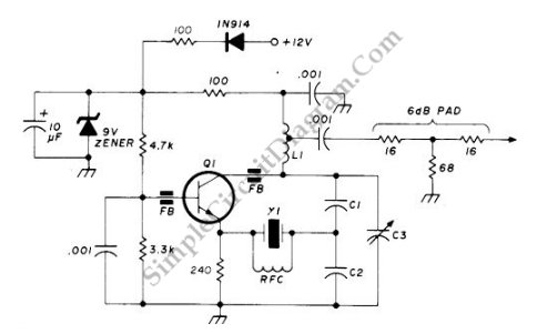
90-125 Mhz Crystal RF Oscillator
This circuit operates at a frequency range of 90-125 MHz and is particularly useful for VHF/UHF converters. It provides an output power of 5 to 15 mW. The circuit can utilize high-quality fifth- or seventh-over-tone crystal types. A ferrite bead...
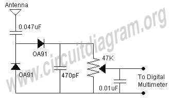
field strength meter fsm
A field strength meter circuit is a valuable device for measuring the RF output of any transmitter or for experimenting with different antennas connected to the transmitter. The operation of the field strength meter (FSM) is straightforward; it converts RF...
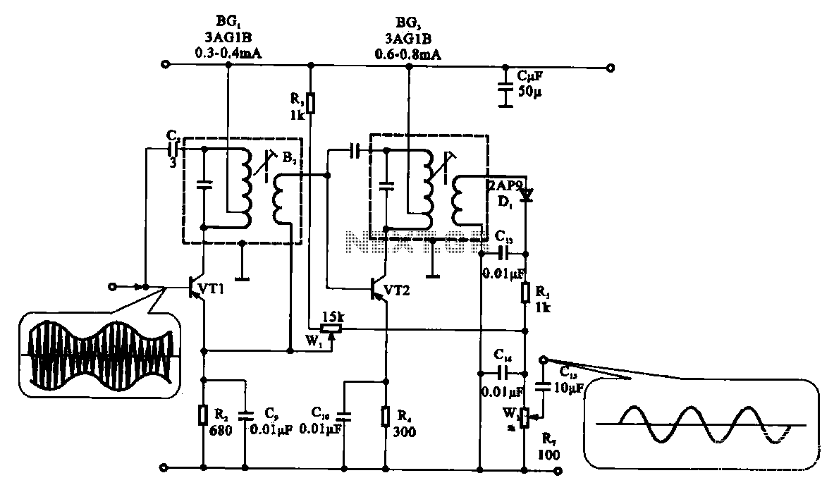
Radio harmonic detection circuit
The demodulation and detection circuit is a radio AM intermediate frequency (IF) signal amplifier that performs two-stage detection using diode Dr. It extracts the audio signal from the IF carrier detection and subsequently sends it to the power amplifier stage....
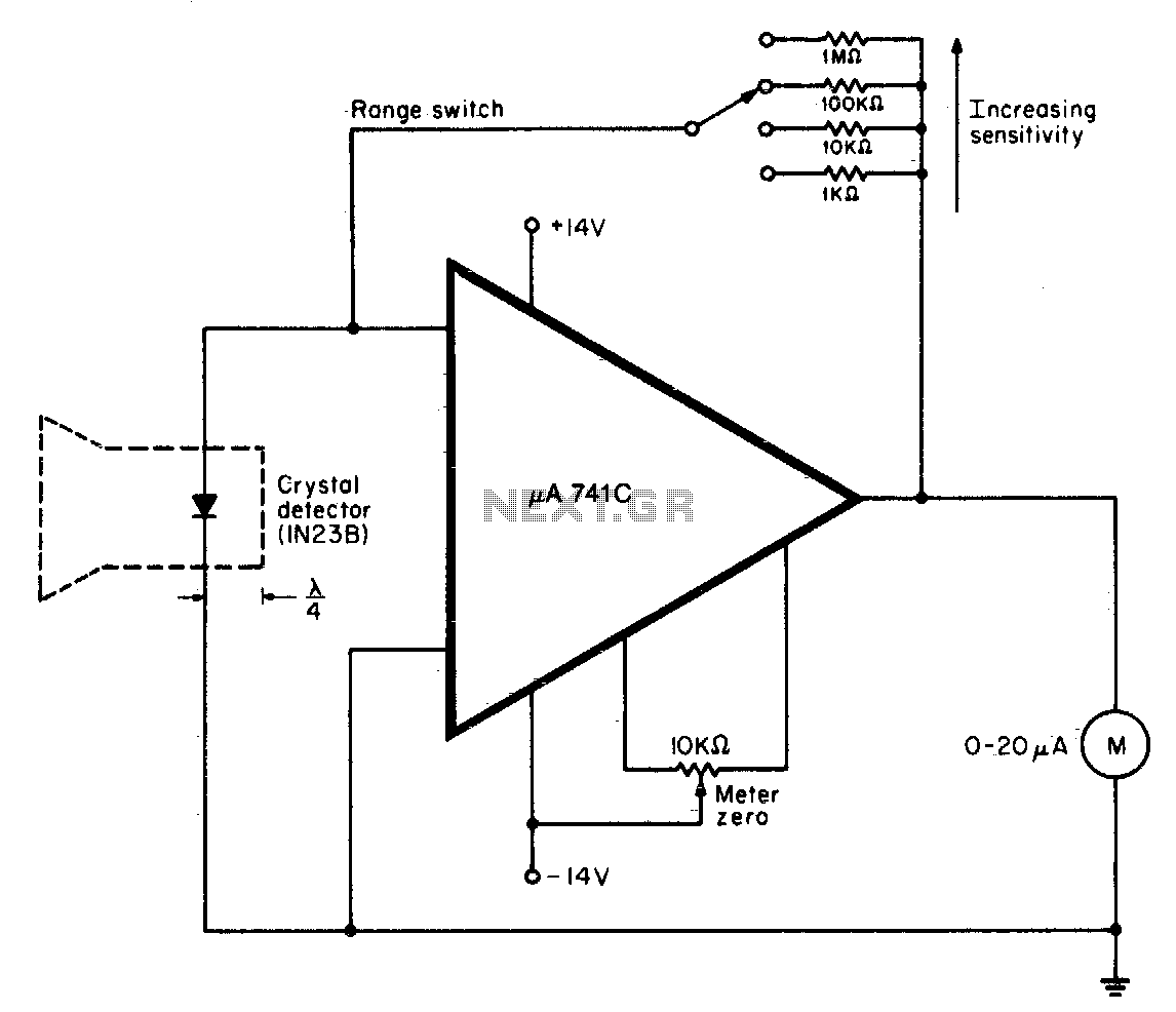
Low cost microwave field strength meter
A waveguide directs energy onto a crystal detector during operation. The diode utilized is designed for X-band operation. The waveguide consists of a 1-inch piece of plastic tubing with flared ends. The plastic surface is treated with an electroless copper...
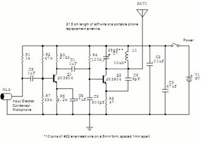
Wireless Car AlarmCircuit With 2N3904 Transistor
The following circuit illustrates a Wireless Car Alarm Circuit Schematic Diagram. Features include the ability to detect sounds within a 20-meter radius, a 1/16 wavelength antenna, and the capability to transmit radio signals up to 2 kilometers. Q1 serves as...
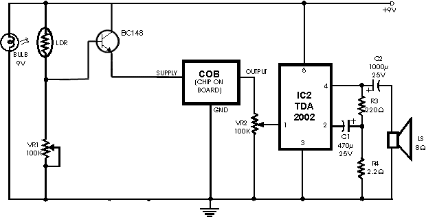
Electronic Mini Projects
The Wireless Imaging Intruder Alarm application allows home security smartphones to detect and send pictures of burglars directly to personal cell phones, PDAs, or computers within seconds of a break-in at homes or businesses when the owner is away. Code...
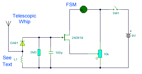
Field Strength Meter
This circuit is a wideband signal strength meter designed to respond to small variations in RF energy within the VHF spectrum. It is capable of detecting AM or FM modulation as well as a simple carrier wave. The circuit measures...
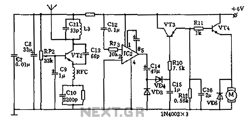
Homemade wireless remote control circuit diagram
The homemade wireless remote control circuit diagram illustrates a motor remote control transmitter circuit. The circuit utilizes a 555 timer along with resistors R1, R2, RP1, diodes VD1, VD2, and capacitor C1 to create a variable duty cycle astable oscillator....
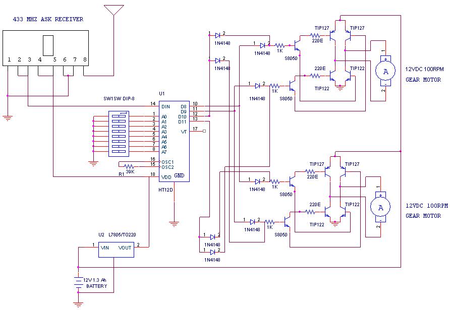
Remote Operated Spy Robot Circuit
A remote-operated spy robot circuit can be controlled using a wireless remote controller. It captures audio and video information from the surroundings and transmits this data to a remote station via RF signals, with a maximum range of 125 meters,...