


fm antenna booster circuit
#FM antenna
#RF amplifier
#2SC2570
#VHF/UHF
#tuned preamplifier
#distant reception
#antenna booster
#FM stations
#RF signal
#printed circuit
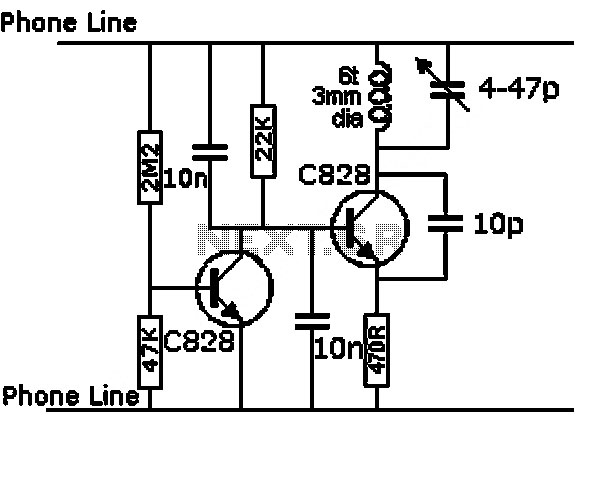
Description: This is a low-cost FM antenna booster designed to enhance reception of programs from distant FM stations. The FM antenna booster circuit features a common-emitter tuned RF preamplifier utilizing the VHF/UHF transistor 2SC2570 (C2570). The schematic illustrates the configuration of the simple FM antenna booster. The circuit should be assembled on a high-quality printed circuit board. Input/output trimmers (VC1/VC2) should be adjusted for optimal gain. The input coil L1 consists of four turns of 20 SWG enameled copper wire, wound slightly spaced over a 5mm diameter former, with a tap at the first turn from the ground lead side. Coil L2 is similar to L1 but contains only three turns. The pin configuration of the 2SC2570 transistor is indicated in the FM antenna booster schematic.
The FM antenna booster circuit is designed to amplify weak radio frequency signals received from distant FM stations, improving audio clarity and reception quality. The core component, the 2SC2570 transistor, operates as a common-emitter amplifier, providing significant gain to the incoming RF signals. This transistor is suitable for VHF/UHF applications, making it ideal for FM reception.
The circuit layout should prioritize minimizing interference and ensuring stable operation. The use of a high-quality printed circuit board (PCB) is essential to reduce parasitic capacitance and inductance, which can adversely affect performance. The input and output trimmers (VC1 and VC2) allow for fine-tuning of the circuit to achieve maximum gain, accommodating variations in signal strength and frequency.
Coil L1, with its four turns of 20 SWG enameled copper wire, serves as the input inductor, which is crucial for tuning the circuit to the desired frequency. The spacing of the windings is important for maintaining the coil's inductance and minimizing losses. The tap on L1 enables the circuit to adjust its input impedance, optimizing the signal transfer from the antenna to the amplifier. Coil L2, with three turns, acts as a coupling inductor, further enhancing the signal amplification process.
The pin configuration of the 2SC2570 transistor should be carefully followed to ensure proper connections and functionality. The circuit may also benefit from additional components such as bypass capacitors to stabilize the power supply and improve overall performance. Proper grounding techniques should be employed to minimize noise and improve signal integrity.
In summary, the FM antenna booster circuit is a straightforward yet effective solution for enhancing FM signal reception, making it an excellent project for electronics enthusiasts and professionals alike.This is a low cost fm antenna booster that can be used to listen to program from distant FM stations clearly. The antenna fm booster circuit comprises a common-emitter tuned RF preamplifier wired around VHF/UHF transistor 2SC2570 (C2570).
This is the schematic of the simple FM Antenna Booster. Assemble the circuit on a good quality of printed circ uit board. Adjust input/output trimmers (VC1/VC2) for maximum gain. Input coil L1 consists of four turns of 20SWG enameled copper wire (slightly space wound) over 5mm diameter former. It is tapped at the first turn from ground lead side. Coil L2 is similar to L1, but has only three turns. Pin configuration of transistor 2SC2570 is shown in the fm antenna booster schematic.
The FM antenna booster circuit is designed to amplify weak radio frequency signals received from distant FM stations, improving audio clarity and reception quality. The core component, the 2SC2570 transistor, operates as a common-emitter amplifier, providing significant gain to the incoming RF signals. This transistor is suitable for VHF/UHF applications, making it ideal for FM reception.
The circuit layout should prioritize minimizing interference and ensuring stable operation. The use of a high-quality printed circuit board (PCB) is essential to reduce parasitic capacitance and inductance, which can adversely affect performance. The input and output trimmers (VC1 and VC2) allow for fine-tuning of the circuit to achieve maximum gain, accommodating variations in signal strength and frequency.
Coil L1, with its four turns of 20 SWG enameled copper wire, serves as the input inductor, which is crucial for tuning the circuit to the desired frequency. The spacing of the windings is important for maintaining the coil's inductance and minimizing losses. The tap on L1 enables the circuit to adjust its input impedance, optimizing the signal transfer from the antenna to the amplifier. Coil L2, with three turns, acts as a coupling inductor, further enhancing the signal amplification process.
The pin configuration of the 2SC2570 transistor should be carefully followed to ensure proper connections and functionality. The circuit may also benefit from additional components such as bypass capacitors to stabilize the power supply and improve overall performance. Proper grounding techniques should be employed to minimize noise and improve signal integrity.
In summary, the FM antenna booster circuit is a straightforward yet effective solution for enhancing FM signal reception, making it an excellent project for electronics enthusiasts and professionals alike.This is a low cost fm antenna booster that can be used to listen to program from distant FM stations clearly. The antenna fm booster circuit comprises a common-emitter tuned RF preamplifier wired around VHF/UHF transistor 2SC2570 (C2570).
This is the schematic of the simple FM Antenna Booster. Assemble the circuit on a good quality of printed circ uit board. Adjust input/output trimmers (VC1/VC2) for maximum gain. Input coil L1 consists of four turns of 20SWG enameled copper wire (slightly space wound) over 5mm diameter former. It is tapped at the first turn from ground lead side. Coil L2 is similar to L1, but has only three turns. Pin configuration of transistor 2SC2570 is shown in the fm antenna booster schematic.
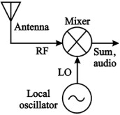
Autodyne Circuit
An Autodyne circuit integrates three functions typically found in separate stages of an RF Receiver into a single circuit. These three stages are the RF amplifier, the Mixer, and the Local Oscillator, which are usually interconnected. In a standard receiver,...
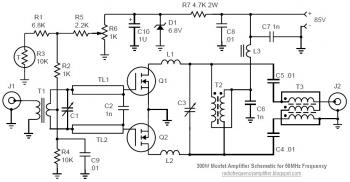
50mhz 300w mosfet amplifier circuit
An RF power amplifier is an electronic amplifier used to convert a low-power radio-frequency signal into a larger signal of significant power, typically for driving the antenna of a transmitter. It is optimized for high efficiency, high output power (P1dB)...
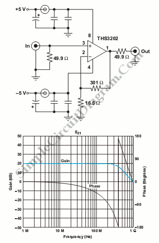
Wideband RF Amplifier
This circuit consists of wideband RF amplifiers that utilize current-feedback components such as the THS3202. The THS3202 was selected for its fast slew rate and wide bandwidth. The amplifier voltage gain of this circuit is 20, while the stage voltage...
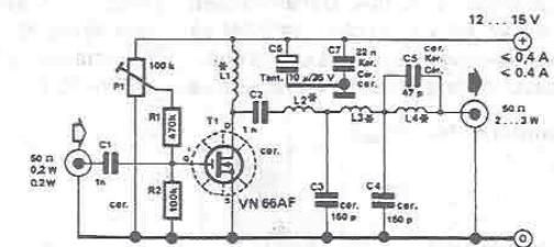
RF amplifier circuit diagram
By using this RF amplifier, small power transmitters of 200 mW can be upgraded to reasonable power transmitters, ranging between 2 and 3 W. The circuit is straightforward. The output filter network suppresses noise by at least 55 dB. The...
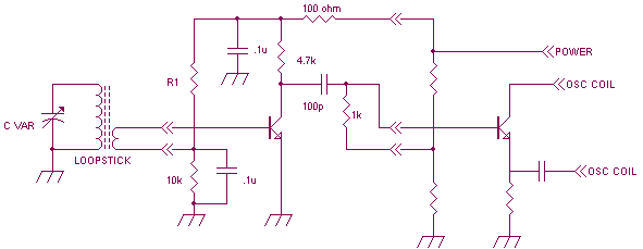
AM RF Amp for Internal Antennas
The author described assembling this circuit on a 1"*1" perf board, I actually laid out a small PC board with excellent results. In this era of surface mount components, I think a much smaller version can be laid out on...
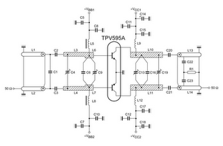
tv power amplifier schematic
TV RF Power Amplifier 14W. This RF power amplifier operates within the frequency range of 470 - 860 MHz, covering UHF Band IV and V, and delivers an output power of 14 Watts with an input power of 1.5 Watts....
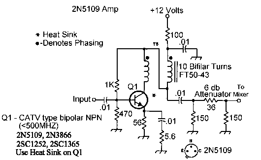
Circuit RF Amplifier
One of the most notable RF amplifiers documented is Wes Hayward's post-mixer amplifier in the Progressive Communications Receiver. It is recognized as a highly effective high-level RF amplifier, operating with a standing current of 50 mA, which allows it to...
1 500-W Rf Amplifier
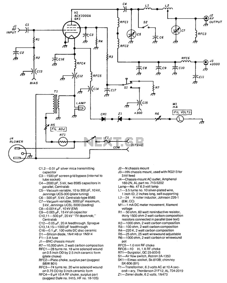
The frequency range of this amplifier is 1.8 to 54 MHz. The required RF drive for full output is approximately 30 W. The grid compartment (Rl, R2, RFC4, RFC5) must be shielded from other circuitry, particularly the output circuitry. Capacitors...
4 watt 900mhz rf amplifier
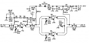
This RF amplifier circuit delivers a power output of 4 Watts at a frequency of 900 MHz. It utilizes Wilkinson power dividers in the base and collector circuits of transistors Q2 and Q3. Two SD1853 driver application transistors are paralleled...