


LOW COST SOLAR RADIO SPECTROGRAPH
#solar
#spectrograph
#analog to digital converter
#RF
#PC games port
#transistor
#measurement
#instrumentation
#wireless
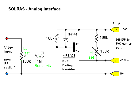
Description: The analog interface is a straightforward analog-to-digital converter that accepts the analog video output from the RF/IF board and converts it into a format that can be read by a PC games port. The joystick input of the games port effectively translates a resistance ranging from 0 to 100k ohms into a binary number from 0 to 255. The interface transistor presents itself to the PC as a variable resistance, with its value approximately proportional to the input voltage. Although the proportionality is not linear, it can still be utilized as a relative value or calibrated if a high-quality signal generator is available, though calibration is not strictly necessary. It is essential to configure the interface according to the output values received from the RF board. This setup process is detailed later. The eight data outputs of register one are employed to tune the radiospectrograph across the frequency band. These outputs are directed to the digital-to-analog converter interface to produce a voltage varying from 2 to 28 volts, which is applied to the tuning pin of the RF tuner. The two least significant bits of register three are used to select either the low band (VHF-Lo) or the high band (VHF-Hi) of the RF tuner. Asserting bit 0 selects VHF-Lo, while asserting bit 1 selects VHF-Hi. It is important to note that both bits 0 and 1 must not be asserted simultaneously. Additionally, the hardware inverts the values presented by the software to these two register bits. A small QBASIC program can be used to cycle the parallel port data byte from 0 to 255, which sets the maximum and minimum voltages output by the digital-to-analog converter (sweep generator). The program is named `DACTEST.BAS` and produces a sawtooth ramp. The code must be executed in DOS mode to ensure direct access to the parallel port without delays. When the parallel port is connected to the DAC and powered, the DAC output should be connected to an oscilloscope to observe the waveform, which should display a sawtooth pattern. The gain and offset controls in the DAC should be adjusted to ensure the waveform ramps between 2 volts minimum and 28 volts maximum, thus calibrating the DAC. The next major calibration involves the analog interface. The voltage applied to the input of this circuit from the VCR RF section depends on the characteristics of the intermediate frequency (IF) amplifier and the subsequent demodulator/detector. Older units typically use several discrete transistor amplifying stages to achieve the necessary high gain, with a discrete germanium diode serving as the detector. In such cases, when there is no input to the RF section (e.g., antenna terminals terminated by a 75-ohm resistor), the output from the diode detector is approximately zero. As the input signal increases, the output voltage may rise to one or two volts. More modern VCRs generally utilize an integrated circuit amplifier for both the IF amp and demodulator, often resulting in a resting voltage well above zero. The output DC level for the prototype SOLRAS is measured at a frequency of 70 MHz as a function of signal input to the antenna. A second program, `STIKTEST.BAS`, is used to test the calibration of the games port joystick input, displaying joystick input values on the screen. The first control to adjust is the Hi Set variable resistor.
The analog interface circuit operates as a bridge between the RF/IF board output and the PC games port, facilitating the conversion of analog signals into digital representations. The core of this interface is a transistor that acts as a variable resistor, adjusting its resistance based on the incoming voltage, which is critical for accurate signal processing. The non-linear relationship between input voltage and resistance must be accounted for during calibration, especially when interfacing with varying signal types from different RF sources.
The digital-to-analog converter (DAC) plays a pivotal role in tuning the RF tuner by generating a precise voltage output that corresponds to the desired frequency. The configuration of the DAC is essential, requiring careful adjustment of both the gain and offset to ensure the output voltage remains within the specified range. The calibration process involves connecting the DAC to an oscilloscope, where the generated waveform can be observed and adjusted accordingly.
The RF tuner’s operational bands are selected through register three, with a clear delineation between VHF-Lo and VHF-Hi. This selection mechanism is critical for ensuring that the tuner operates within the appropriate frequency range, avoiding potential signal interference or degradation. The inversion of bit values in the hardware necessitates careful programming to ensure the correct operational state is achieved.
The calibration of the analog interface must also consider the characteristics of the RF section of the VCR, particularly the type of amplifiers and detectors used. The output characteristics will vary significantly between older discrete component designs and modern integrated solutions, impacting the overall sensitivity and accuracy of the analog interface. The ability to measure and adjust these parameters is vital for maintaining signal integrity and achieving optimal performance in signal processing applications.
In summary, the design and calibration of the analog interface and associated components are critical for ensuring reliable operation and accurate signal conversion in applications involving RF signals and digital processing.The analog interface is a very simple analog to digital converter which accepts the analog video output of the RF/IF board and puts it into a form that can be read by a PC Games port. The joystick input of the games port essentially converts a resistance in the range 0 to 100k ohms into a binary number from 0 to 255.
The interface transistor looks to the PC as such a variable resistance, whose value is roughly proportional to the input voltage. The proportionality is not linear, but then neither is the receiver output. It can be used as a relative value, or it can be calibrated if a good quality signal generator is available. However, this is not necessary. It is necessary however, to set up the interface in accordance with the output values that it will receive from the RF board.
This process is described later. The eight data outputs of register one are used to tune the radiospectrograph across the frequency band. These are fed to the digital to analog converter interface as previously described to produce a voltage that varies from 2 to 28 volts.
This is applied to the tuning pin of the RF tuner. The two least significant bits of register 3 are used to select either low band (VHF-Lo) or the high band (VHF-Hi) of the RF tuner. Asserting bit 0 selects VHF-Lo, while asserting bit 1 selects VHF-Hi. Note that both bits 0 and 1 must not be asserted together. Also realise that the hardware does an inversion of the values presented by the software to these two register bits.
A small QBASIC program that cycles the parallel port data byte from 0 to 255 can be used to set the max and min voltages output by the digital to analog converter (sweep generator). The code is listed below. `File name DACTEST. BAS `DAC test `produces a sawtooth ramp dly = 0 `increase to increase step delay PRINT "Press ESC to end test" DO FOR i% = 0 TO 255 `value for DAC OUT 888, i% `output to LPT1 GOSUB Delay `wait a while NEXT i% `increment number LOOP WHILE INKEY$ <> CHR$(27) `press escape to exit END Delay: FOR zz = 0 TO dly NEXT zz RETURN This program must be run in DOS mode (not in a DOS window under WINDOWS).
Only in this mode are you sure of direct access to the parallel port without delays. With the parallel port connected to the DAC and power applied, connect the output of the DAC to an oscilloscope. Activate the program and observe the oscilloscope trace. It should be a sawtooth waveform. Adjust both the gain and the offset controls in the DAC to ensure that the waveform ramps between 2 volts minimum and 28 volts maximum.
The DAC is then calibrated. The next major calibration is the analog interface. The voltage applied to the input of this circuit from the VCR RF section will depend on the nature of the intermediate frequency (IF) amplifier and the subsequent demodulator/detector. If this is a really old unit it will probably employ several discrete transistor amplifying stages to achieve the required high gain.
The detector in these cases is usually a discrete germanium diode. When there is no input to the RF section (eg antenna terminals terminated by a 75 ohm resistor) the output from the diode detector will be approximately zero. As the input signal increases, the output voltage will rise to maybe a volt or two. A more modern VCR will usually employ an integrated circuit amplifier as both the IF amp and demodulator.
These often have a resting voltage well above zero. The table below indicates the output DC level for the prototype SOLRAS as a function of signal input to the antenna. This was measured at a frequency of 70 MHz. `Filename STIKTEST. BAS `Testing calibration of games port joystick input SCREEN 7 `large characters for visibility DO `set up an infinite loop a = STICK(0) `sample joystick A - X input LOCATE 12, 20 `then display in the PRINT a `middle of the screen LOOP WHILE INKEY$ <> CHR$(27) `ESCape to exit loop END The first control to adjust is the Hi Set variable resist
The analog interface circuit operates as a bridge between the RF/IF board output and the PC games port, facilitating the conversion of analog signals into digital representations. The core of this interface is a transistor that acts as a variable resistor, adjusting its resistance based on the incoming voltage, which is critical for accurate signal processing. The non-linear relationship between input voltage and resistance must be accounted for during calibration, especially when interfacing with varying signal types from different RF sources.
The digital-to-analog converter (DAC) plays a pivotal role in tuning the RF tuner by generating a precise voltage output that corresponds to the desired frequency. The configuration of the DAC is essential, requiring careful adjustment of both the gain and offset to ensure the output voltage remains within the specified range. The calibration process involves connecting the DAC to an oscilloscope, where the generated waveform can be observed and adjusted accordingly.
The RF tuner’s operational bands are selected through register three, with a clear delineation between VHF-Lo and VHF-Hi. This selection mechanism is critical for ensuring that the tuner operates within the appropriate frequency range, avoiding potential signal interference or degradation. The inversion of bit values in the hardware necessitates careful programming to ensure the correct operational state is achieved.
The calibration of the analog interface must also consider the characteristics of the RF section of the VCR, particularly the type of amplifiers and detectors used. The output characteristics will vary significantly between older discrete component designs and modern integrated solutions, impacting the overall sensitivity and accuracy of the analog interface. The ability to measure and adjust these parameters is vital for maintaining signal integrity and achieving optimal performance in signal processing applications.
In summary, the design and calibration of the analog interface and associated components are critical for ensuring reliable operation and accurate signal conversion in applications involving RF signals and digital processing.The analog interface is a very simple analog to digital converter which accepts the analog video output of the RF/IF board and puts it into a form that can be read by a PC Games port. The joystick input of the games port essentially converts a resistance in the range 0 to 100k ohms into a binary number from 0 to 255.
The interface transistor looks to the PC as such a variable resistance, whose value is roughly proportional to the input voltage. The proportionality is not linear, but then neither is the receiver output. It can be used as a relative value, or it can be calibrated if a good quality signal generator is available. However, this is not necessary. It is necessary however, to set up the interface in accordance with the output values that it will receive from the RF board.
This process is described later. The eight data outputs of register one are used to tune the radiospectrograph across the frequency band. These are fed to the digital to analog converter interface as previously described to produce a voltage that varies from 2 to 28 volts.
This is applied to the tuning pin of the RF tuner. The two least significant bits of register 3 are used to select either low band (VHF-Lo) or the high band (VHF-Hi) of the RF tuner. Asserting bit 0 selects VHF-Lo, while asserting bit 1 selects VHF-Hi. Note that both bits 0 and 1 must not be asserted together. Also realise that the hardware does an inversion of the values presented by the software to these two register bits.
A small QBASIC program that cycles the parallel port data byte from 0 to 255 can be used to set the max and min voltages output by the digital to analog converter (sweep generator). The code is listed below. `File name DACTEST. BAS `DAC test `produces a sawtooth ramp dly = 0 `increase to increase step delay PRINT "Press ESC to end test" DO FOR i% = 0 TO 255 `value for DAC OUT 888, i% `output to LPT1 GOSUB Delay `wait a while NEXT i% `increment number LOOP WHILE INKEY$ <> CHR$(27) `press escape to exit END Delay: FOR zz = 0 TO dly NEXT zz RETURN This program must be run in DOS mode (not in a DOS window under WINDOWS).
Only in this mode are you sure of direct access to the parallel port without delays. With the parallel port connected to the DAC and power applied, connect the output of the DAC to an oscilloscope. Activate the program and observe the oscilloscope trace. It should be a sawtooth waveform. Adjust both the gain and the offset controls in the DAC to ensure that the waveform ramps between 2 volts minimum and 28 volts maximum.
The DAC is then calibrated. The next major calibration is the analog interface. The voltage applied to the input of this circuit from the VCR RF section will depend on the nature of the intermediate frequency (IF) amplifier and the subsequent demodulator/detector. If this is a really old unit it will probably employ several discrete transistor amplifying stages to achieve the required high gain.
The detector in these cases is usually a discrete germanium diode. When there is no input to the RF section (eg antenna terminals terminated by a 75 ohm resistor) the output from the diode detector will be approximately zero. As the input signal increases, the output voltage will rise to maybe a volt or two. A more modern VCR will usually employ an integrated circuit amplifier as both the IF amp and demodulator.
These often have a resting voltage well above zero. The table below indicates the output DC level for the prototype SOLRAS as a function of signal input to the antenna. This was measured at a frequency of 70 MHz. `Filename STIKTEST. BAS `Testing calibration of games port joystick input SCREEN 7 `large characters for visibility DO `set up an infinite loop a = STICK(0) `sample joystick A - X input LOCATE 12, 20 `then display in the PRINT a `middle of the screen LOOP WHILE INKEY$ <> CHR$(27) `ESCape to exit loop END The first control to adjust is the Hi Set variable resist
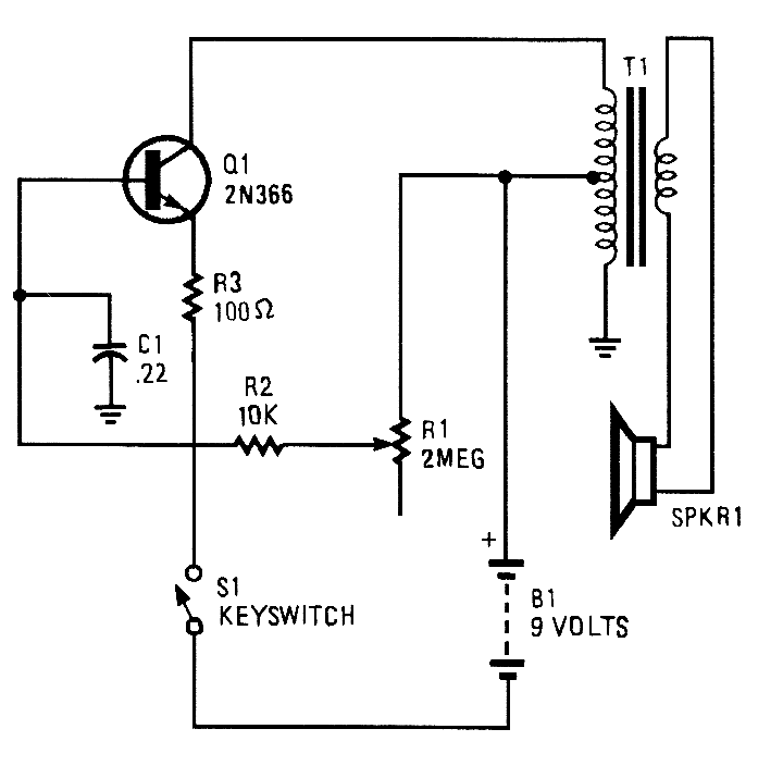
SINGLE TRANSISTOR CODE PRACTICE OSCILLATOR
A 2N366 is configured as an audio feedback oscillator using an audio transformer. Adjust R1 for proper operation and the desired audio note.
The circuit utilizes a 2N366 transistor, which is a general-purpose NPN transistor, serving as the primary active component...
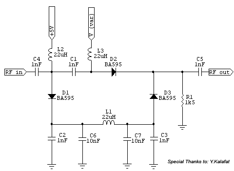
RF Signal Attenuator up to 30dB for 1MHz - 500MHz Input
This is a PIN diode-based RF signal attenuator circuit that operates with input frequencies ranging from 1 MHz to 500 MHz. PIN diodes are among the most commonly used components in RF applications.
The RF signal attenuator circuit utilizing PIN diodes...
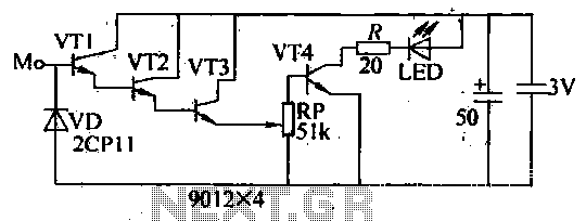
Blanket internal measurement circuit disconnection
The internal disconnection circuit for a blanket operates on the principle of induction. It includes a wire approximately 2 cm in length that senses the proximity of a charged mains power source. When the sensing wire is close to the...
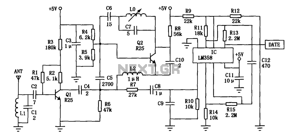
DF data transmission module and the super-regenerative receiver module
The DF data transmission module operates at a frequency of 315 MHz and utilizes a surface acoustic wave (SAW) resonator for frequency stabilization, ensuring high frequency stability. The frequency drift remains minimal, at only 3 x 10^-6, across a temperature...
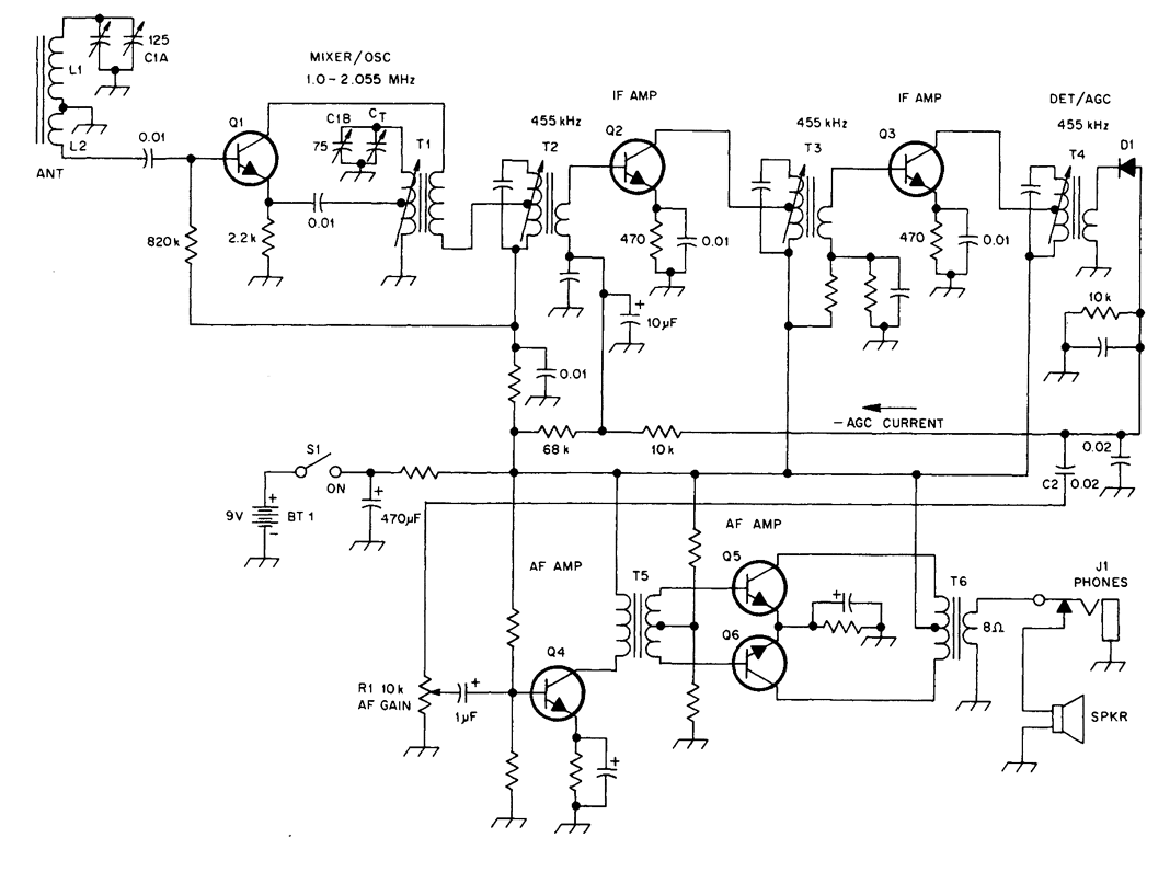
TRANSISTORIZED AM RADIO
The schematic illustrates a standard AM radio circuit utilizing NPN transistors. This generic circuit does not provide specific values for all components, serving instead as a reference point for experimenters to begin their projects.
The schematic of a typical transistor AM...
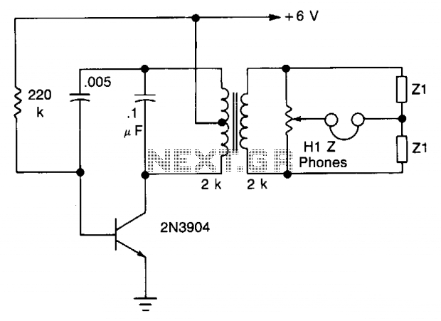
Bridge circuit
The transistor is configured as an audio oscillator, utilizing an audio transformer in the collector. The secondary winding is connected to a linear potentiometer. The ratio between the two sections of the potentiometer from the slider is proportional to the...
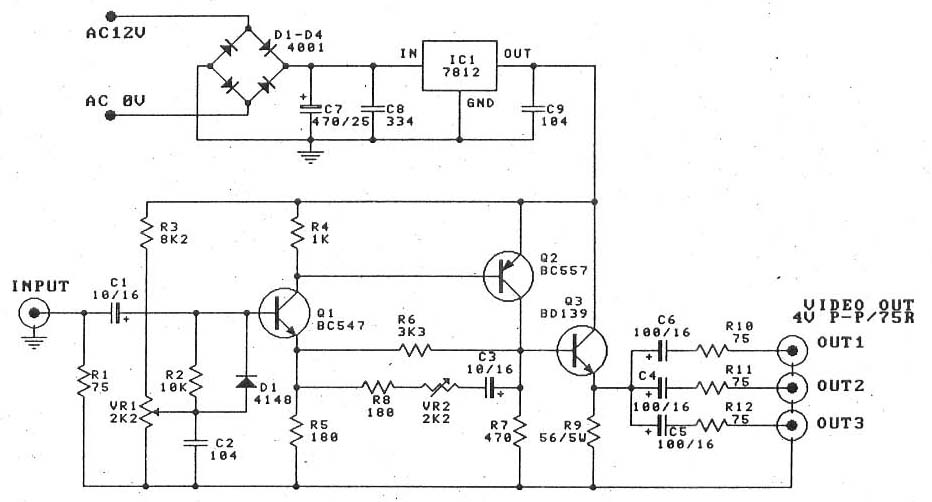
Video amplifier splitter by transistor BD137-BC547-BC557
This is a video amplifier circuit or video splitter circuit, designed to strengthen video signals. It compensates for signal loss and is...
The video amplifier circuit serves as a crucial component in video signal distribution systems, ensuring that the integrity and...

Transistor Amplifier Circuit with Diagram for 12 Watts
A simple transistor amplifier circuit diagram and schematic that can be used as a 12-watt audio transistor amplifier. An operational amplifier (op-amp) integrated circuit (IC) is used to produce the required gain.
This circuit is designed to amplify audio signals, making...

speak memory
Mike Licht confesses to the transistor-related misadventures of his youth. The pocket transistor radio is considered essential to mid-20th century American pop music, but its significance extends beyond music itself; it played a vital role in shaping conversations and thoughts...