


LSB Conversion of RT321 and RT320 HF Sets
#HF sets
#LSB conversion
#USB operation
#Amateur radio
#sideband inversion
#RT320
#RT321
#SSB generation
#1.7500 MHz IF
#Clansman
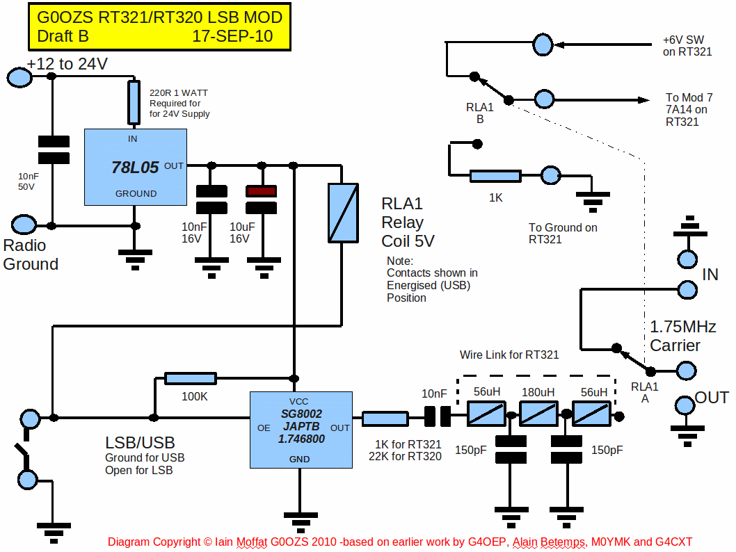
Description: The RT320 and RT321 Clansman HF sets are designed exclusively for Upper Side Band (USB) operation. This design choice conflicts with the Amateur radio convention, which typically utilizes Lower Side Band (LSB) on frequencies below 10 MHz. In both radios, the Intermediate Frequency (IF) for Single Side Band (SSB) generation is set at 1.7500 MHz, resulting in a sideband inversion between the IF and the antenna. Thus, LSB at the IF translates to USB at the output, while USB at the IF results in LSB at the output. The IF filter passband for SSB is approximately 0.2 to 3.0 kHz below the IF frequency, effectively blocking the 1.7500 MHz carrier and allowing pure LSB to be transmitted. To achieve LSB at the output, one would need to either replace the filter with a USB variant or adjust the carrier frequency below the filter passband. The latter method was first detailed by Dr. Andrew Smith G4OEP in an article available on the VMARS Manuals website. This modification requires a crystal oscillator set at 3.2 kHz below the original 1.7500 MHz frequency, resulting in a new frequency of 1.7468 MHz. However, sourcing a 1.7468 MHz crystal can pose challenges due to size and cost, prompting the exploration of alternative, more economical solutions. One such solution involves using a programmable oscillator, which consists of a VHF crystal and a Phase-Locked Loop (PLL) to generate arbitrary programmed frequencies. This oscillator can replace the transistor CIO in the G4OEP circuit, provided a suitable 5V TTL power supply is available and the output is adequately filtered to be compatible with the radio. A recommended oscillator is the SG8002-JAPTB, which operates within a frequency range of 1 to 125 MHz and offers a temperature tolerance of 50 ppm (equating to a potential deviation of up to 87.5 Hz, which is acceptable for SSB but may impact narrow data modes). Typically, samples at room temperature have demonstrated a deviation of within 5 ppm of the programmed frequency. The SG8002 is housed in a J-leaded plastic package, comparable in size to an 8-pin DIP operational amplifier. It is important to note that the Output Enable is active high, a detail that was misinterpreted in the original suggested circuit diagram, as pointed out by G4CXT and John Moore. The last purchase of these components was priced at £1.36 each for a quantity of 50, with an additional programming fee of £25 and £10 for shipping, resulting in an effective unit cost of £2.06 for programmed devices. It should be noted that no personal modifications have been made to the sets, as they remain functional, but a bulk purchase of SG8002s has been coordinated, with several users successfully implementing the conversion on both the RT320 and RT321 models. Critical factors for successful modification include disabling the built-in 1.7500 MHz CIO when utilizing LSB or employing a changeover relay with sufficient isolation to prevent a 3.2 kHz tone from appearing on the transmitted LSB signal. Additionally, the output level of the 1.7468 MHz signal must be adjusted to match that of the original 1.7500 MHz carrier. The RT320 modification follows the G4OEP guidelines, with the 1.7468 MHz transistor CIO being substituted with the SG8002. A small 5V voltage regulator is necessary, powered by the 12V supply, as there is no 5V logic supply present in this model. The 5V TTL output from the SG8002 requires filtering to produce a sine wave output. A suitable filter design includes R1 (1 kΩ) in series with L1 (56 μH), followed by C1 (150 pF) in shunt, L2 (180 μH) in series with C2 (150 pF) in shunt, and L3 (56 μH) in series. The RT321's 1.7500 MHz CIO is accessible on SMB socket 7SK1 at the bottom of module 7 (1st LO), with appropriate power and control signals available on the module's pins. The internal circuit of module 7 features a TTL output with 10 nF and 1 kΩ in series, indicating that the same components should work effectively with the SG8002 output. The frequency switch inputs for module 7, which are required to select LSB for 3 and 7 MHz, can be found on pins 16, 15, 24, 23, 21, and 22 of 7a. Further investigation is needed to decode these inputs to MHz, building on the earlier work of Terry G4BFS, Alain Betemps, Mike Hyers, Colin Guy, Iain M0YMK, and Andy G4JAC.The RT320 and RT321 Clansman HF sets are designed for Upper Side Band (USB) operation only. This conflicts with the Amateur radio convention which is to use LSB on bands below 10MHz. In both radios the IF used for SSB generation is 1. 7500 MHz and there is a sideband inversion between the IF and the antenna. So LSB at the IF comes out as USB and US B at the IF comes out as LSB. The IF filter passband for SSB is roughly 0. 2 to 3. 0KHz below the IF frequency so the 1. 7500MHz carrier is blocked leaving pure LSB. To get LSB at the output it would be necessary either to change the filter to a USB one or to move the carrier below the filter passband. The latter approach is what was first documented by Dr. Andrew Smith G4OEP in his excellent article now available on the VMARS Manuals web site: A crystal at 3.
2KHz below the original 1. 7500MHz = 1. 7468MHz is needed for the G4OEP LSB modification. Unfortunately the size and cost of a 1. 7468MHz crystal is now somewhat of a problem and other cheaper solutions have been sought. One is to use a programmable oscillator comprising a VHF crystal and a PLL to generate programmed arbitary frequencies. Such an oscillator can replace the transistor CIO in the G4OEP circuit provided a suitable (5 V TTL) power supply is available and the output is adequately filtered and at a level compatible with the radio.
A suitable oscillator is the SG8002-JAPTB which covers 1 to 125MHz and has a 0 to 70 degrees C tolerance of 50ppm (so would be up to 87. 5Hz off - not a problem for SSB but would affect narrow data modes). At room temperature samples have measured within 5ppm of the programmed frequency. Physically it is a J-Leaded plastic package about the size of an 8 pin DIP op-amp. The data sheet is at Important Note: The Output Enable is active high - I misread the data sheet when preparing the original suggested circuit diagram.
This has been pointed out by G4CXT and John Moore. Last time I bought some they were £1. 36 each for 50, with a programming charge of £25 and carriage of £10 making an effective price of £2. 06 plus postage for programmed units. I should prefix this section by stating that I have not personally modified any sets (on the basis that mine aint broke so I will wait til I really need LSB or have need to open them for repairs).
I have coordinated a bulk purchase of SG8002s and several people have had success with the conversion on both RT320 and RT321. Critical factors for success are to inhibit the 1. 7500MHz built in CIO when using LSB or have a changeover relay with good isolation (otherwise it appears as a 3.
2KHz tone on the transmitted LSB signal) and to set the output level of the 1. 7468MHz signal to match the original 1. 75MHz carrier. The RT320 modification is as described by G4OEP except that the 1. 7468MHz transistor CIO is replaced by the SG8002. A small 5V voltage regulator is required which should be fed from the 12V supply, since no 5V logic supply exists in this set. The 5V TTL output of the SG8002 must be filtered to get a sine wave output. A suitable filter design is: R1 1K series L1 56uH series C1 150pF shunt L2 180uH series C2 150pF shunt L3 56uH series (This diagram needs a monospaced font like courier) o-10nF-R1-L1-L2-L3-o | | From SG8002 C1 C2 To Mixer | | o-o The RT321 1.
75MHz CIO appears on SMB socket 7SK1 at the bottom of module 7 (1st LO) and suitable power and control signals also exist on pins of this module. The circuit internally to module 7 is a TTL output with 10nF and 1K in series so the same components in series with the SG8002 output should be satisfactory.
Decoding the frequency switch inputs to module 7 to select LSB for 3 and 7MHz - these are on 7a pins 16, 15, 24, 23, 21 and 22 in order. I dont have a decode for these to MHz so further investigation is needed. This page is based on earlier work by Terry G4BFS, Alain Betemps, Mike Hyers, Colin Guy, Iain M0YMK, Andy G4JAC, John Mo
2KHz below the original 1. 7500MHz = 1. 7468MHz is needed for the G4OEP LSB modification. Unfortunately the size and cost of a 1. 7468MHz crystal is now somewhat of a problem and other cheaper solutions have been sought. One is to use a programmable oscillator comprising a VHF crystal and a PLL to generate programmed arbitary frequencies. Such an oscillator can replace the transistor CIO in the G4OEP circuit provided a suitable (5 V TTL) power supply is available and the output is adequately filtered and at a level compatible with the radio.
A suitable oscillator is the SG8002-JAPTB which covers 1 to 125MHz and has a 0 to 70 degrees C tolerance of 50ppm (so would be up to 87. 5Hz off - not a problem for SSB but would affect narrow data modes). At room temperature samples have measured within 5ppm of the programmed frequency. Physically it is a J-Leaded plastic package about the size of an 8 pin DIP op-amp. The data sheet is at Important Note: The Output Enable is active high - I misread the data sheet when preparing the original suggested circuit diagram.
This has been pointed out by G4CXT and John Moore. Last time I bought some they were £1. 36 each for 50, with a programming charge of £25 and carriage of £10 making an effective price of £2. 06 plus postage for programmed units. I should prefix this section by stating that I have not personally modified any sets (on the basis that mine aint broke so I will wait til I really need LSB or have need to open them for repairs).
I have coordinated a bulk purchase of SG8002s and several people have had success with the conversion on both RT320 and RT321. Critical factors for success are to inhibit the 1. 7500MHz built in CIO when using LSB or have a changeover relay with good isolation (otherwise it appears as a 3.
2KHz tone on the transmitted LSB signal) and to set the output level of the 1. 7468MHz signal to match the original 1. 75MHz carrier. The RT320 modification is as described by G4OEP except that the 1. 7468MHz transistor CIO is replaced by the SG8002. A small 5V voltage regulator is required which should be fed from the 12V supply, since no 5V logic supply exists in this set. The 5V TTL output of the SG8002 must be filtered to get a sine wave output. A suitable filter design is: R1 1K series L1 56uH series C1 150pF shunt L2 180uH series C2 150pF shunt L3 56uH series (This diagram needs a monospaced font like courier) o-10nF-R1-L1-L2-L3-o | | From SG8002 C1 C2 To Mixer | | o-o The RT321 1.
75MHz CIO appears on SMB socket 7SK1 at the bottom of module 7 (1st LO) and suitable power and control signals also exist on pins of this module. The circuit internally to module 7 is a TTL output with 10nF and 1K in series so the same components in series with the SG8002 output should be satisfactory.
Decoding the frequency switch inputs to module 7 to select LSB for 3 and 7MHz - these are on 7a pins 16, 15, 24, 23, 21 and 22 in order. I dont have a decode for these to MHz so further investigation is needed. This page is based on earlier work by Terry G4BFS, Alain Betemps, Mike Hyers, Colin Guy, Iain M0YMK, Andy G4JAC, John Mo
frx 2001
Software, applications, and programming resources. Amateur radio and travel. Stereogram art.
The provided content outlines various topics of interest, including software applications and programming resources, amateur radio, travel, and stereogram art. Each of these areas represents a distinct field with its...
The Second W9VES
The amateur radio call sign W9VES has been assigned to only two individuals, of whom the second is the author. The first holder was the author's maternal uncle, Phil Simmons, and the author enjoys amateur radio in his memory. By...
The Crystalizer
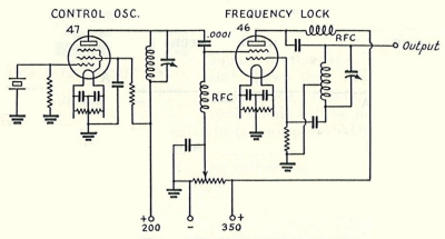
A classic amateur radio transmitter topology, known as the oscillator-amplifier (often referred to as master oscillator, power amplifier, or MOPA), utilizes one tube for frequency control and another for RF power amplification. In its quartz-crystal-controlled form, it typically allows operation...
AB4YD Amateur Radio Page
This project was inspired by a series of QST articles by Hayward, W1PH. The design is based on his April 1962 article, "Have You Tried 160 Lately." The rig features a simple, single-band configuration utilizing 6V6 tubes with regulated voltages,...
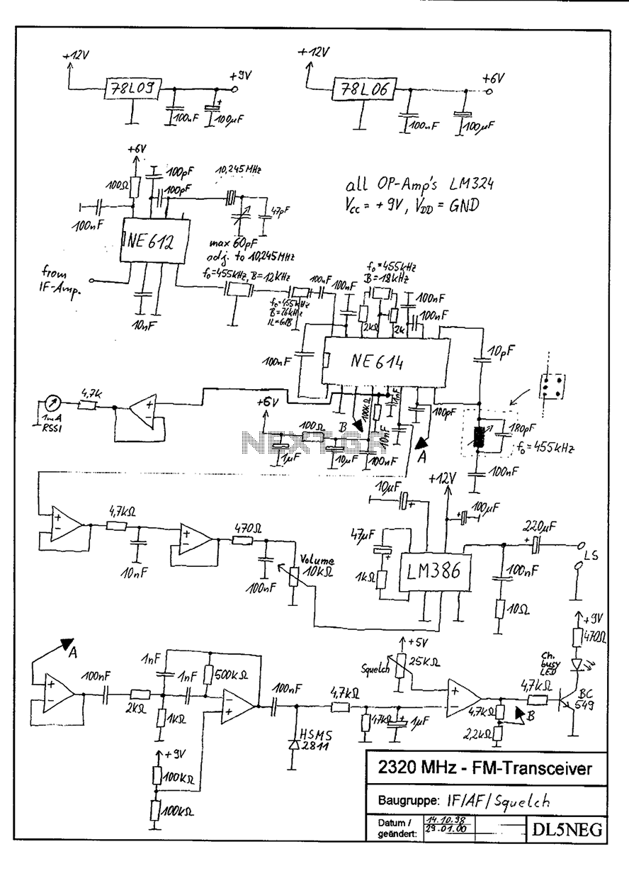
high-quality 2.3 GHz Amateur Radio Transceiver
The receiver is a triple superheterodyne receiver with two phase-locked loop (PLL) guided local oscillators. The first local oscillator (LO) operates at 2.1 GHz and can be adjusted in increments of 500 kHz, down-converting the received signal to a frequency...
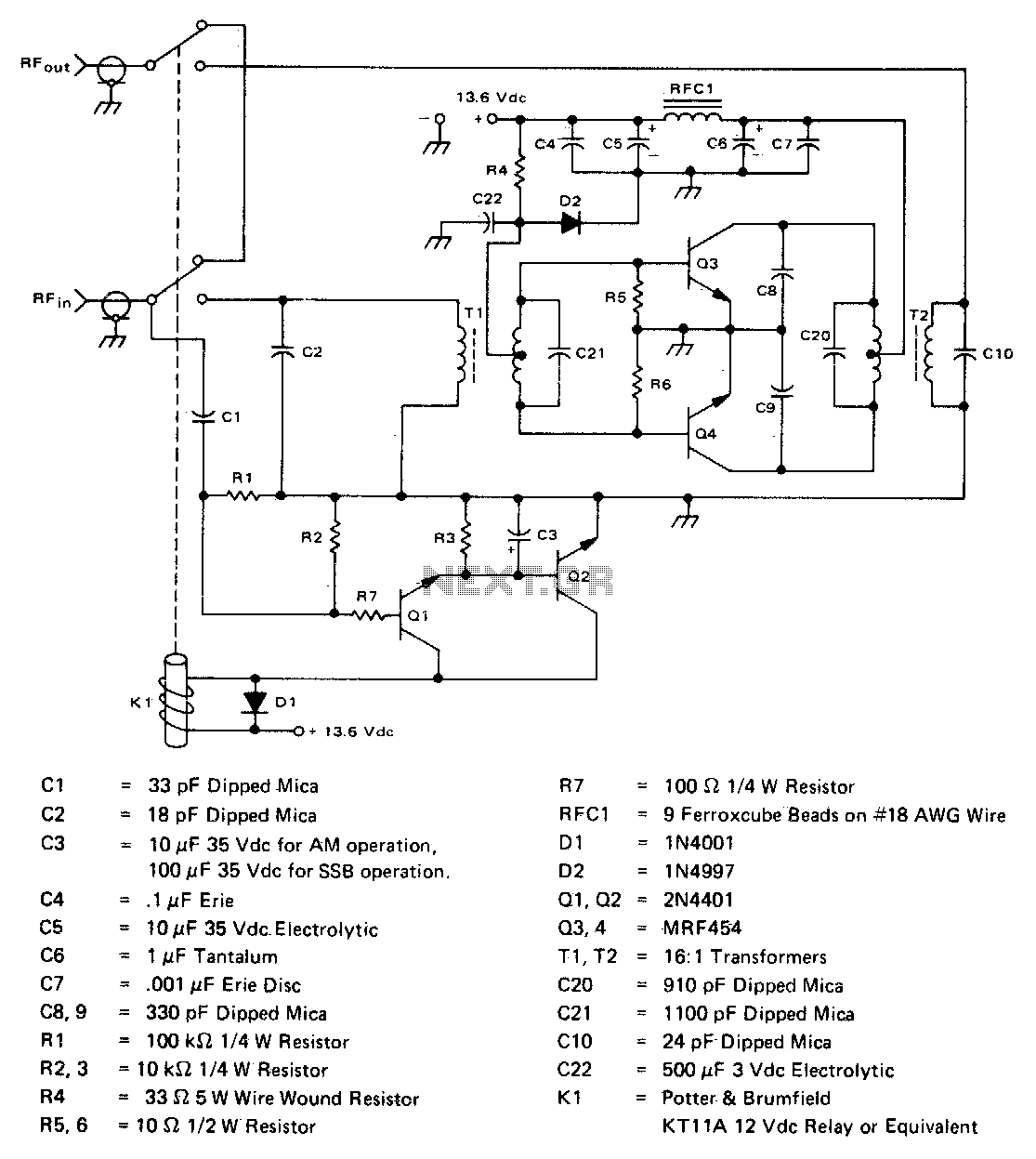
140W amateur radio linear amplifier 2-30Mhz
This inexpensive, easy-to-construct amplifier utilizes two MRF454 devices. It is specified for an 80 W power output with a 5 W input drive at a frequency of 30 MHz and operates on a 12 V DC supply.
The amplifier circuit is...
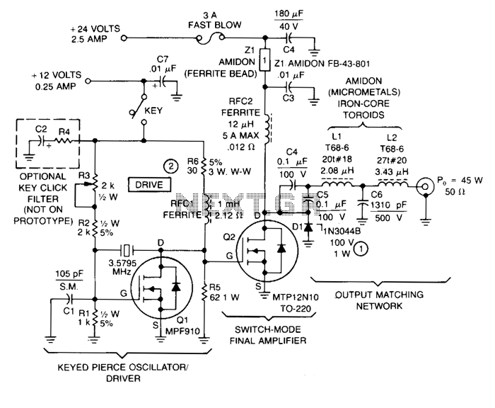
80M-amateur-radio-transmitter
This transmitter comprises a keyed crystal oscillator/driver and a high-efficiency final amplifier, both utilizing a TMOS Power FET as the active component. The total cost of components is under $20, and no specialized construction skills or circuit boards are necessary....
Amateur Radio Projects
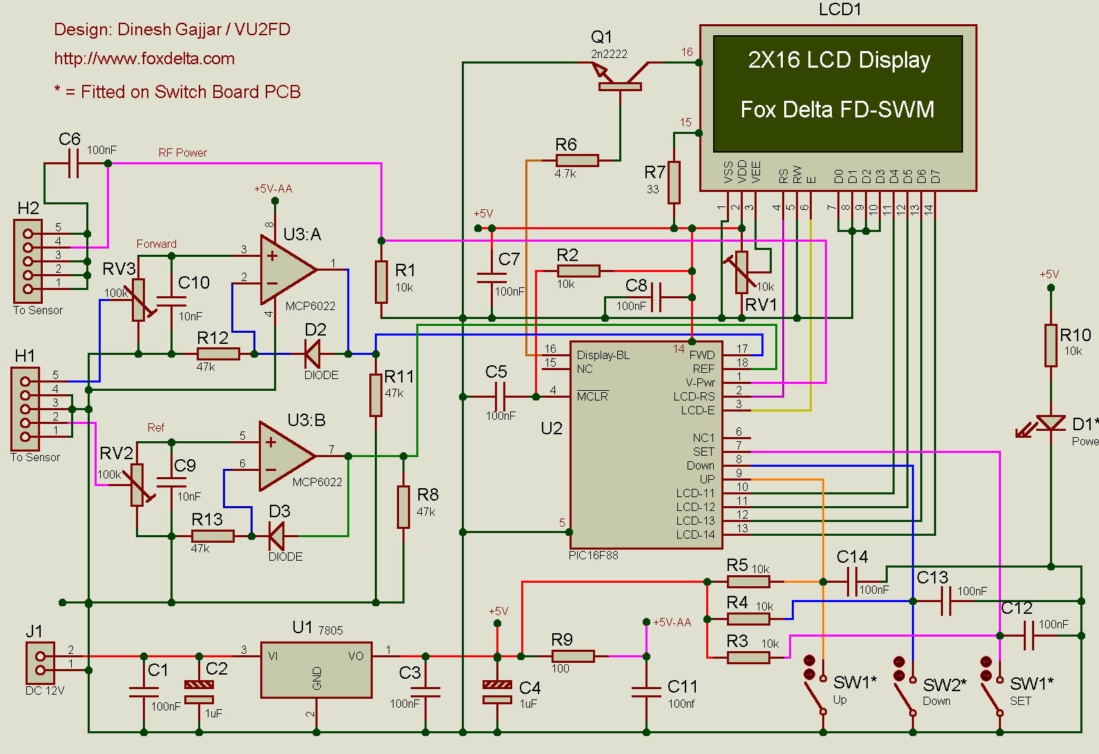
The development of this interface for Echolink took some time. It utilizes the PIC16F84A microcontroller and accepts external DTMF signals from a radio. The latest version, Foxecho-k7, provides complete isolation between the radio and the PC and features automatic gain...
Amateur Radio
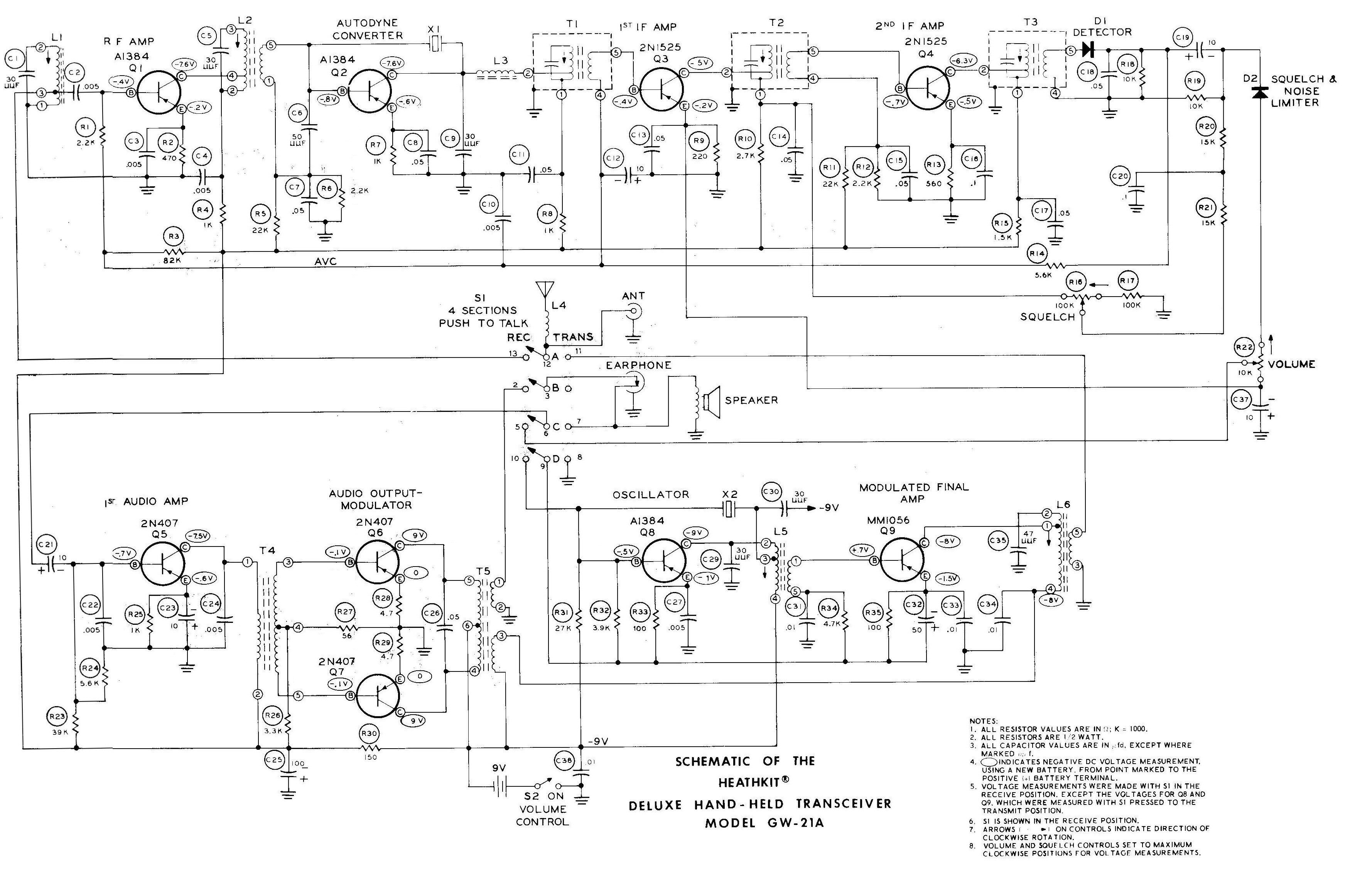
This device features crystal-controlled transmitters and tunable superregenerative receivers equipped with RF preamplifiers, designed for operation on the 2, 6, or 10 meter amateur bands. The highly sensitive receivers can detect signals as low as 1 microvolt, providing complete quieting...