


MC28332 Single Chip VHF Narrowband FM Transmitter Application Circuit
#VHF
#FM transmitter
#narrowband
#frequency multiplier
#crystal oscillator
#RF buffer
#transistor
#frequency doubler
#frequency tripler
#MC2833
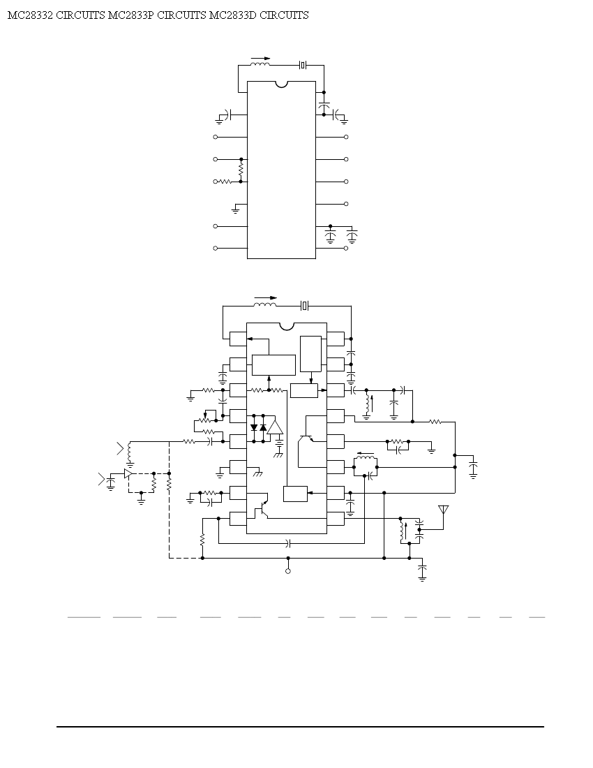
Description: Crystal X1 operates in fundamental mode and is calibrated for parallel resonance with a load capacitance of 32 pF. The final output frequency is produced through frequency multiplication within the MC2833 integrated circuit (IC). The RF output buffer at Pin 14 and the Q2 transistor function as a frequency tripler and doubler, respectively, in the 76 MHz and 144.6 MHz transmitters.
Crystal X1 is a critical component in RF transmitter designs, particularly in applications requiring precise frequency generation. Operating in fundamental mode, it ensures stable oscillation characteristics essential for maintaining signal integrity. The calibration for a 32 pF load capacitance allows for optimal performance, ensuring that the crystal resonates accurately at its designated frequency.
The MC2833 IC plays a pivotal role in the frequency multiplication process. It takes the fundamental frequency generated by Crystal X1 and multiplies it to achieve the desired output frequencies. The architecture of the MC2833 is designed to support various frequency multiplication techniques, enabling efficient signal processing within the transmitter.
The RF output buffer located at Pin 14 is essential for interfacing the output of the MC2833 with the subsequent stages of the transmitter circuit. This buffer amplifies the output signal, ensuring that it can drive the next stage without significant loss of power or signal quality. Additionally, the Q2 transistor is employed as a frequency doubler, effectively doubling the frequency of the output signal, while the frequency tripler configuration allows for the generation of higher frequencies, specifically at 76 MHz and 144.6 MHz.
In summary, the combination of Crystal X1, the MC2833 IC, and the associated RF output buffer and transistor configurations facilitates the generation of stable and precise RF signals, making it suitable for various communication applications, including amateur radio and other RF transmission systems.Crystal X1 is fundamental mode, calibrated for parallel resonance with a 32 pF load. The final output frequency is generated by frequency multiplication within the MC2833 IC. The RF output Buffer (Pin 14) and Q2 Transistor are used as a frequency tripler and doubler, respectively, in the 76 and 144. 6 MHz Transmitters
Crystal X1 is a critical component in RF transmitter designs, particularly in applications requiring precise frequency generation. Operating in fundamental mode, it ensures stable oscillation characteristics essential for maintaining signal integrity. The calibration for a 32 pF load capacitance allows for optimal performance, ensuring that the crystal resonates accurately at its designated frequency.
The MC2833 IC plays a pivotal role in the frequency multiplication process. It takes the fundamental frequency generated by Crystal X1 and multiplies it to achieve the desired output frequencies. The architecture of the MC2833 is designed to support various frequency multiplication techniques, enabling efficient signal processing within the transmitter.
The RF output buffer located at Pin 14 is essential for interfacing the output of the MC2833 with the subsequent stages of the transmitter circuit. This buffer amplifies the output signal, ensuring that it can drive the next stage without significant loss of power or signal quality. Additionally, the Q2 transistor is employed as a frequency doubler, effectively doubling the frequency of the output signal, while the frequency tripler configuration allows for the generation of higher frequencies, specifically at 76 MHz and 144.6 MHz.
In summary, the combination of Crystal X1, the MC2833 IC, and the associated RF output buffer and transistor configurations facilitates the generation of stable and precise RF signals, making it suitable for various communication applications, including amateur radio and other RF transmission systems.Crystal X1 is fundamental mode, calibrated for parallel resonance with a 32 pF load. The final output frequency is generated by frequency multiplication within the MC2833 IC. The RF output Buffer (Pin 14) and Q2 Transistor are used as a frequency tripler and doubler, respectively, in the 76 and 144. 6 MHz Transmitters

Transistor Amplifier Circuit with Diagram for 12 Watts
A simple transistor amplifier circuit diagram and schematic that can be used as a 12-watt audio transistor amplifier. An operational amplifier (op-amp) integrated circuit (IC) is used to produce the required gain.
This circuit is designed to amplify audio signals, making...
Frequency Doubler
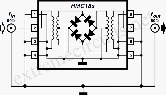
When working with frequencies ranging from 850 MHz to 4 GHz, a frequency multiplier may be necessary. The HMC 187, HMC 188, and HMC 189 frequency doublers could be suitable solutions. These devices offer isolation performance that attenuates the input...
the simplest fm transmitter ever made
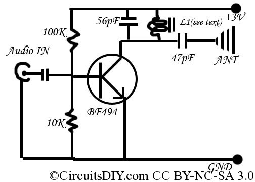
This is a simple and inexpensive FM transmitter. The circuit operates at a low voltage using a CR2025 3V battery with low current consumption. The total size of this FM transmitter, including the battery but excluding the antenna, is smaller...
Crystal Oscillator - Parallel Resonant
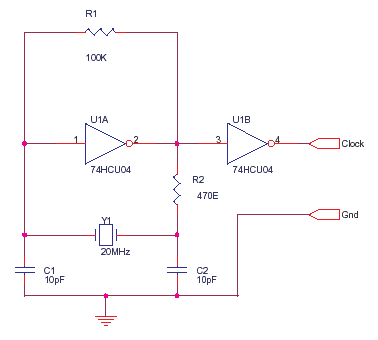
The 74HCU04 is a chip designed for specific circuit applications, while the HCT variant may not be suitable for such configurations. Capacitors C1 and C2 can be utilized up to 33pF, and resistor R2 can be adjusted to achieve the...
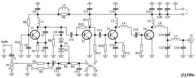
3 Watt FM transmitter
Connect two 24 V / 3 W bulbs in parallel to the output and set the right frequency on PLL. Now turn on the transmitter. You should tune it on a receiver. Maybe you might stretch coils of the L1....
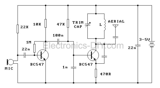
FM Transmitter
This FM transmitter is one of the simplest and most basic designs that can be built while still providing a useful transmitting range. Despite its small component count and 3V operating voltage, it is surprisingly powerful, capable of transmitting over...
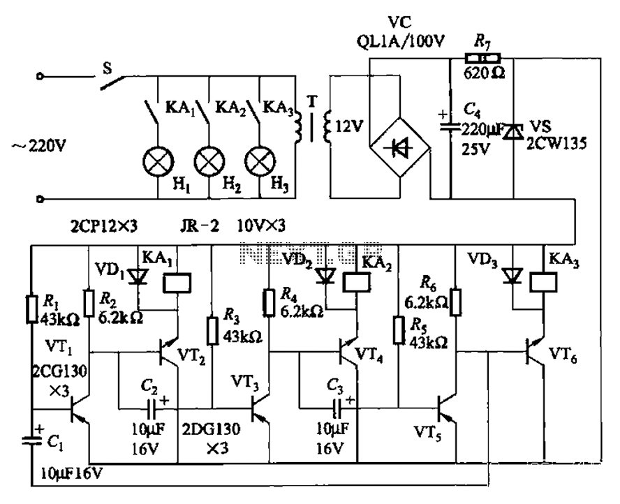
Alternately flashing lights chain multiple sets of high-power circuit 2
The transistors VTi, VT3, and VTs, along with the RC components, form three distinct multi-resonator oscillators. The oscillation frequency levels are dependent on the values of Ri, R3, Rs, and Cl, as well as Cz and C3s.
The circuit comprises three...
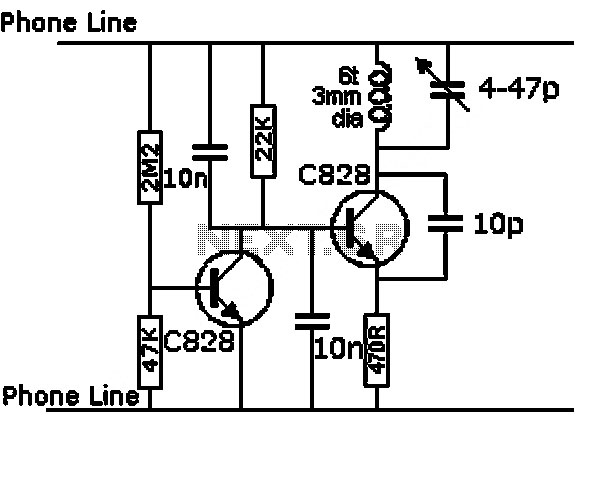
Low Capacitance High Impedance Amplifier Circuit Using Transistor
This series-feedback configuration of components provides a high input impedance and stable, wide-band gain video amplifier suitable for general-purpose applications. Below is the schematic representation of the circuit.
The described video amplifier circuit employs a series-feedback topology, which is instrumental in...
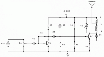
1.5 Watt FM Transmitter circuit
This project was completed successfully, achieving the desired frequency and strength. For assistance, please reach out for support in resolving any issues.
The project involves the design and implementation of an electronic circuit that operates at a specified frequency and strength,...