


zener Floating Voltage to Bias a P-Channel Mosfet without Exceeding Source-Gate Max Voltage
#P-Channel MOSFET
#Zener diode
#voltage bias
#freewheeling diode
#back EMF
#coil driving
#square pulses
#high-side switching
#circuit protection
#negative voltage handling
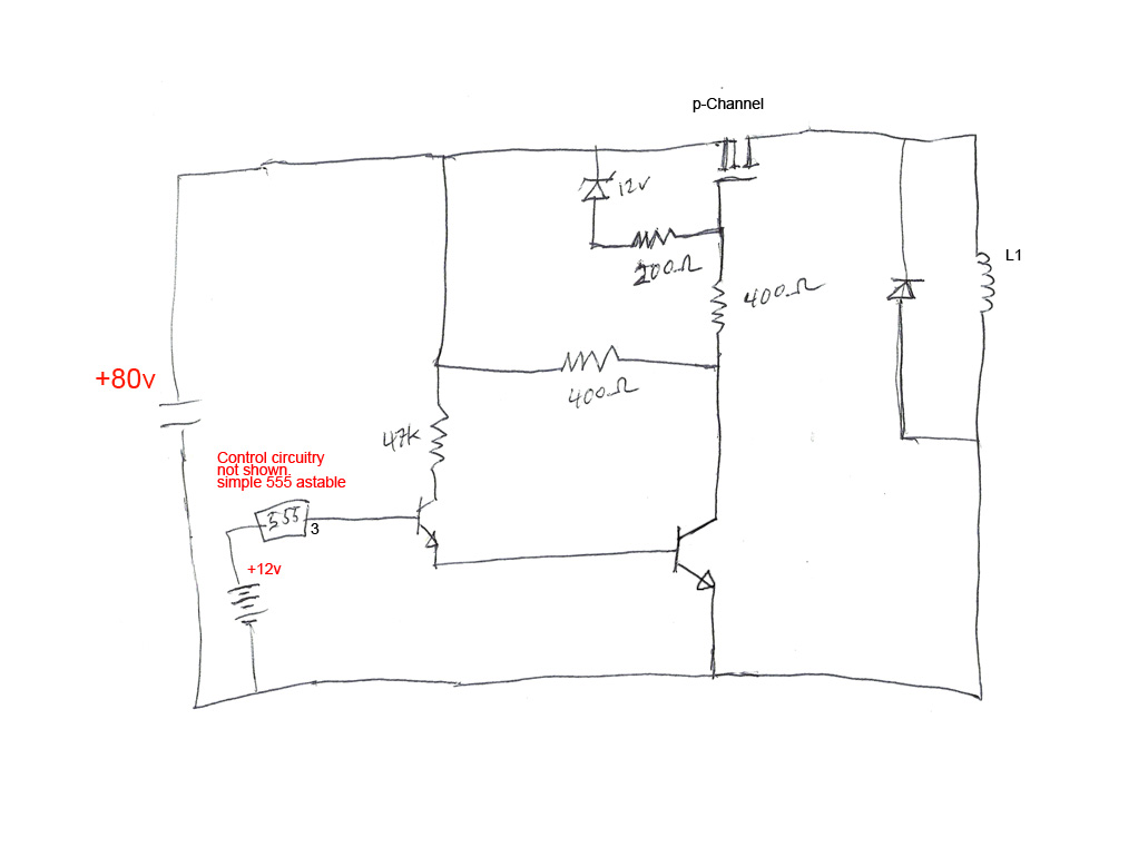
Description: The circuit's premise involves powering an L1 coil with square pulses. A freewheeling diode is included to manage the back EMF field collapse, thereby protecting the circuitry. Previous experiments indicated that using an N-channel MOSFET on the high side of the coil is ineffective due to the significant negative voltage during back EMF collapse, which causes the gate at zero volts to inadvertently turn on. Although BJTs were tested and resolved the issue, they tend to overheat. The preference is to utilize MOSFETs for their capability to handle high current with minimal resistance. Consequently, a P-channel MOSFET has been adopted in the circuit design. This design, while straightforward, introduces complexity as it aims to accommodate varying high voltages in the main circuit, exemplified by 80 volts but potentially adjustable. To ensure the circuit remains indifferent to the actual main power voltage, a resistor network has been integrated to supply the necessary gate voltage from the power source. A 555 timer and BJTs are employed to pull down the gate voltage for MOSFET activation. A critical aspect of the design is preventing the gate voltage from dropping to 0V, which would create an 80-volt differential between the Source and Gate, risking MOSFET damage. The solution involves incorporating a 12-volt Zener diode, with resistance values adjusted so that if the gate voltage exceeds 12 volts below the source, the diode will reverse bias, restoring the gate voltage. The gate voltage should stabilize around 68 volts when the power supply is at 80 volts, provided the BJT remains biased on. When the BJT turns off, the gate will return to 80 volts, thereby deactivating the MOSFET.
The circuit operates by utilizing a P-channel MOSFET to switch the current through the L1 coil, which generates magnetic fields when energized. The inclusion of a freewheeling diode is critical for safeguarding the MOSFET and other components from voltage spikes caused by the inductive load during the off state. The design incorporates a 555 timer configured in astable mode to generate the square pulse signal required to energize the coil. The output from the 555 timer is connected to the base of the BJTs, which act as switches to control the gate voltage of the P-channel MOSFET.
The resistor network plays a vital role in ensuring that the gate voltage is maintained at a safe level relative to the source voltage. This network is designed to deliver an adequate gate voltage that allows the MOSFET to switch effectively without exceeding its maximum gate-source voltage rating. The use of the 12-volt Zener diode is a protective measure that prevents the gate voltage from dropping too low, thus avoiding the risk of damaging the MOSFET. This diode will conduct when the gate voltage approaches 12 volts below the source voltage, thereby clamping the gate voltage and allowing for stable operation across a range of input voltages.
In summary, this circuit design effectively addresses the challenges associated with driving an inductive load using MOSFET technology while ensuring protection against back EMF and maintaining operational integrity across varying power supply conditions. Proper component selection and configuration are crucial for achieving the desired performance and reliability.The premise of the circuit is this: I want to power L1 coil with square pulses. You can see I`ve got a freewheeling diode to handle the back emf field collapse to protect the circuitry. From previous experiments and talking to others on here, I learned that using an N-channel mosfet on the high side of the coil like this doesn`t work because the large negative voltage during the back emf coil collapse puts negative voltage
on the mosfet source which causes the gate (at zero volts) to turn on while the field is collapsing. I experimented with BJTs and they make it easy to fix the problem, but they also get hot. I really want to use mosfets for the ability to pass a lot of current with minimal resistance. So I`ve switched to a P-channel mosfet in the circuit shown. This seems pretty simple but I`m adding a level of complexity. I want to have arbitrarily high voltage in the main circuit - 80volts shown here but it could be more or less. Since the voltage is prone to change in use conditions, the circuit design must be agnostic to the actual main power voltage.
In the 80 volt example shown, since the p-channel mosfet requires 80volts at the gate to turn it off, I have added a small resistor network to supply the required voltage from the power src. You can see I`m using a 555 and some BJT`s to pull down the gate voltage to turn it on. Now the tricky part. From my understanding, I can`t drop the mosfet gate all the way to 0V because that would make an 80volt difference between the Source and the Gate which would destroy it.
I need to make sure the gate drops to about 12 volts less than the Source but drops no further. THe solution I`ve come up with is to add a 12 volt zener diode and adjust the resistances accordingly so once the gate starts to become more than 12 volts less than the source, the diode will reverse bias and bring the gate back up. It should stay right around 68volts if the power supply is 80 volts - as long as the BJT is biased on anyway.
Once the BJT turns off, the gate will recover to 80 volts and shut off the mosfet.
The circuit operates by utilizing a P-channel MOSFET to switch the current through the L1 coil, which generates magnetic fields when energized. The inclusion of a freewheeling diode is critical for safeguarding the MOSFET and other components from voltage spikes caused by the inductive load during the off state. The design incorporates a 555 timer configured in astable mode to generate the square pulse signal required to energize the coil. The output from the 555 timer is connected to the base of the BJTs, which act as switches to control the gate voltage of the P-channel MOSFET.
The resistor network plays a vital role in ensuring that the gate voltage is maintained at a safe level relative to the source voltage. This network is designed to deliver an adequate gate voltage that allows the MOSFET to switch effectively without exceeding its maximum gate-source voltage rating. The use of the 12-volt Zener diode is a protective measure that prevents the gate voltage from dropping too low, thus avoiding the risk of damaging the MOSFET. This diode will conduct when the gate voltage approaches 12 volts below the source voltage, thereby clamping the gate voltage and allowing for stable operation across a range of input voltages.
In summary, this circuit design effectively addresses the challenges associated with driving an inductive load using MOSFET technology while ensuring protection against back EMF and maintaining operational integrity across varying power supply conditions. Proper component selection and configuration are crucial for achieving the desired performance and reliability.The premise of the circuit is this: I want to power L1 coil with square pulses. You can see I`ve got a freewheeling diode to handle the back emf field collapse to protect the circuitry. From previous experiments and talking to others on here, I learned that using an N-channel mosfet on the high side of the coil like this doesn`t work because the large negative voltage during the back emf coil collapse puts negative voltage
on the mosfet source which causes the gate (at zero volts) to turn on while the field is collapsing. I experimented with BJTs and they make it easy to fix the problem, but they also get hot. I really want to use mosfets for the ability to pass a lot of current with minimal resistance. So I`ve switched to a P-channel mosfet in the circuit shown. This seems pretty simple but I`m adding a level of complexity. I want to have arbitrarily high voltage in the main circuit - 80volts shown here but it could be more or less. Since the voltage is prone to change in use conditions, the circuit design must be agnostic to the actual main power voltage.
In the 80 volt example shown, since the p-channel mosfet requires 80volts at the gate to turn it off, I have added a small resistor network to supply the required voltage from the power src. You can see I`m using a 555 and some BJT`s to pull down the gate voltage to turn it on. Now the tricky part. From my understanding, I can`t drop the mosfet gate all the way to 0V because that would make an 80volt difference between the Source and the Gate which would destroy it.
I need to make sure the gate drops to about 12 volts less than the Source but drops no further. THe solution I`ve come up with is to add a 12 volt zener diode and adjust the resistances accordingly so once the gate starts to become more than 12 volts less than the source, the diode will reverse bias and bring the gate back up. It should stay right around 68volts if the power supply is 80 volts - as long as the BJT is biased on anyway.
Once the BJT turns off, the gate will recover to 80 volts and shut off the mosfet.
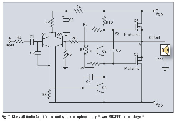
p channel power mosfets approach n channel performance
Utilizing the latest advancements in trench and polar power MOSFET technologies, both trench and polar P-Channel power MOSFETs have been developed that maintain all the characteristics of comparable N-Channel power MOSFETs, including rapid switching, voltage control, ease of paralleling, and...
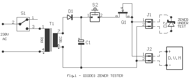
Zener Diode checker
Many times we have found itself in the necessity to use a Zener diode and cannot to know the voltage of operation. Many times we cannot read the characteristics or the type that is written on her. In this case,...
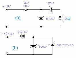
Zener Oscillator circuits
These two circuits are interesting from an academic point of view. Their practical implementation is rather critical and it is not easy to get steady operation. Circuit (a) requires a "cooked" zener: connect it first to a constant current generator,...

How to build a zener diode tester
This circuit is designed to test zener diodes. It connects to a 120V AC line and amplifies the output.
The zener diode testing circuit operates by utilizing a transformer to step down the 120V AC line voltage to a more manageable...
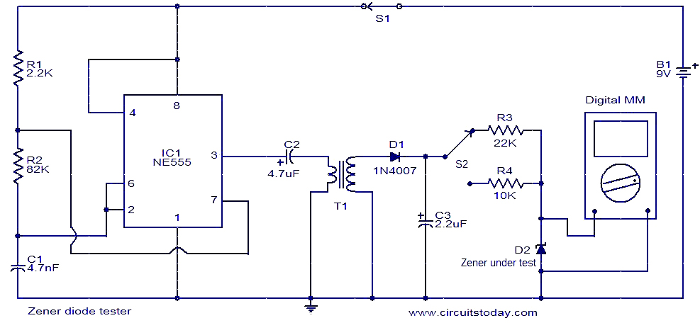
Zener diode tester
This circuit is designed for testing Zener diodes. The NE555 integrated circuit (IC1) is configured as an astable multivibrator, generating a square wave output. This output is transformed into a high voltage alternating current (AC) by transformer T1, with an...
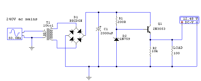
Regulated 12 Volt Supply
This circuit utilizes a 13-volt zener diode, D2, which is responsible for voltage regulation. Approximately 0.7 volts are dropped across the base-emitter junction of the transistors, resulting in a higher current output of 12.3 volts. The circuit is capable of...

henry alc zener
The Automatic Loading Control (ALC) 100 volt 5 watt zener diode in Henry RF amplifiers is known to fail. Initially, it shorts, causing a high voltage (HV) surge, which typically results in the zener blowing open and tripping the main...

Zener Tester schematic
With this simple measuring device can: Determine the Zener voltage up to 25V. The connections of cathode and anode of each diode finding. Check if a diode fails. Silicon, germanium and Schottky diodes distinguish. LED test and the V forward...
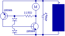
Zener-based solar engine
The capacitor charges until the PNP transistor (here shown as a 2N3906, but you could also use a BC327) receives base current through the Zener and turns on. Then the NPN transistor (here shown as a 2N3904, but you could...