


DQPSK Pi4DemodSync
#DQPSK
#demodulation
#modulation
#data streams
#filters
#differential decoder
#symbol delay
#I and Q channels
#telecommunication
#radio frequency
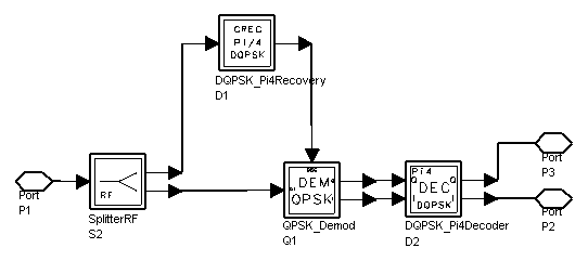
Description: The input and output data streams of the I and Q data channels are presented in a Pi/4DQPSK system operating at a carrier frequency of 990 MHz and a data rate of 48.6 kbits/sec. A notable delay exists between the input and output data signals, attributed to the filters in both the modulator and demodulator, each contributing a delay of 4 Symbol Time seconds, along with the differential decoder adding an additional delay of 1 Symbol Time second. Consequently, the total delay from input to output is 9 Symbol Time seconds, which translates to approximately 370.37 seconds at the specified data rate. The eye patterns of the output data signals are depicted in the Eye Pattern of I and Q Data Signals (carrier recovered using the DQPSK_Pi4Recovery component). In certain applications, it may be necessary to combine the I and Q channel data streams into a single data stream. A clock recovery circuit must be designed to generate an appropriate clock, or alternatively, a clock component can be utilized with the correct phase to sample the I and Q data streams and combine them using the BinaryCombinerClocked component. An example setup for measuring the Bit Error Rate (BER) of the system is illustrated in the Pi/4DQPSK System. Additive white Gaussian noise is introduced into the channel, and a bandpass filter is employed at the input of the demodulator to allow the signal to pass without distortion while eliminating out-of-band noise. A Clock component is used to produce the sampling clock signal, with its phase adjusted by the Delay parameter. This adjustment is made by measuring the delay from the Data component to the output of the DQPSK_Pi4DemodSync component, as referenced in Delay Through Pi/4DQPSK System. The clock is delayed by the total delay plus an additional 0.5 Symbol Time to ensure sampling occurs at the midpoint of the symbol. The input and output data streams are illustrated in the Pi/4DQPSK System, where the input data stream is delayed to align with the output data stream.
In the described Pi/4DQPSK system, the modulation technique utilizes phase-shift keying to encode data onto a carrier wave, effectively allowing for higher data rates within a given bandwidth. The I (in-phase) and Q (quadrature) components are crucial for achieving this encoding, facilitating the transmission of two bits per symbol. The delays introduced by the modulator, demodulator, and differential decoder must be carefully accounted for in the design of the system to ensure accurate signal recovery and minimize errors.
The design of the clock recovery circuit is critical, as it synchronizes the sampling process with the transmitted signal. The clock phase adjustment is essential to align the sampling instances with the optimal points in the data stream, particularly at the midpoint of each symbol, to mitigate the effects of timing jitter and improve the overall performance of the system.
The integration of a bandpass filter at the demodulator's input is a fundamental aspect of the design, as it ensures that only the desired frequency components of the signal are processed, while effectively rejecting noise that could interfere with signal integrity. This filtering process enhances the system's robustness against noise, thereby improving the Bit Error Rate (BER) performance.
In summary, the Pi/4DQPSK system exemplifies a sophisticated approach to digital communication, balancing the complexities of modulation, demodulation, and signal processing to achieve reliable data transmission in the presence of noise. The meticulous design considerations for delays, clock recovery, and filtering are integral to ensuring high-quality performance in practical applications.The input and output data streams of the I and Q data channels are shown in Pi/4DQPSK System: fc=990 MHz, Data rate = 48. 6 kbits/sec. Note the delay between the input and output data signals. This delay is due to the filters in the modulator and demodulator, each of which introduces a delay of 4SymbolTime seconds, and the differential decoder, wh
ich introduces a delay of 1SymbolTime second. Therefore, the delay from input to output is 9SymbolTime seconds, which for a data rate of 48. 6 kbits/sec equals 370. 37 seconds. The eye patterns of the output data signals are shown in Eye Pattern of I and Q Data Signals (carrier recovered using the DQPSK_Pi4Recovery component): fc=990 MHz, Data rate = 48. 6 kbits/sec. For certain applications, the I and Q channel data streams may have to be combined into a single data stream.
The user must design a clock recovery circuit to generate a clock, or else use the clock component with the appropriate phase to sample the I and Q data streams and combine them using the BinaryCombinerClocked component. As an example, a simple setup to measure the BER of the system is shown in Pi/4DQPSK System: fc=990 MHz, Data rate = 48.
6 kbits/sec. Additive white Gaussian noise is introduced in the channel. A bandpass filter is placed at the input to the demodulator that lets the signal through without distortion, but removes the out-of-band noise. In Pi/4DQPSK System: fc=990 MHz, Data rate = 48. 6 kbits/sec a Clock component is used to generate the sampling clock signal. The phase of the clock is adjusted by the Delay parameter of the Clock component. This phase is adjusted by measuring the delay from the Data component to the output of the DQPSK_Pi4DemodSync component; refer to Delay Through Pi/4DQPSK System.
The clock is delayed by the total delay plus an additional time of 0. 5SymbolTime to sample the data at the midpoint of the symbol. The input and output data streams are shown in Pi/4DQPSK System: fc=990 MHz, Data rate = 48. 6 kbits/sec (the input data stream is delayed to align the two data streams).
In the described Pi/4DQPSK system, the modulation technique utilizes phase-shift keying to encode data onto a carrier wave, effectively allowing for higher data rates within a given bandwidth. The I (in-phase) and Q (quadrature) components are crucial for achieving this encoding, facilitating the transmission of two bits per symbol. The delays introduced by the modulator, demodulator, and differential decoder must be carefully accounted for in the design of the system to ensure accurate signal recovery and minimize errors.
The design of the clock recovery circuit is critical, as it synchronizes the sampling process with the transmitted signal. The clock phase adjustment is essential to align the sampling instances with the optimal points in the data stream, particularly at the midpoint of each symbol, to mitigate the effects of timing jitter and improve the overall performance of the system.
The integration of a bandpass filter at the demodulator's input is a fundamental aspect of the design, as it ensures that only the desired frequency components of the signal are processed, while effectively rejecting noise that could interfere with signal integrity. This filtering process enhances the system's robustness against noise, thereby improving the Bit Error Rate (BER) performance.
In summary, the Pi/4DQPSK system exemplifies a sophisticated approach to digital communication, balancing the complexities of modulation, demodulation, and signal processing to achieve reliable data transmission in the presence of noise. The meticulous design considerations for delays, clock recovery, and filtering are integral to ensuring high-quality performance in practical applications.The input and output data streams of the I and Q data channels are shown in Pi/4DQPSK System: fc=990 MHz, Data rate = 48. 6 kbits/sec. Note the delay between the input and output data signals. This delay is due to the filters in the modulator and demodulator, each of which introduces a delay of 4SymbolTime seconds, and the differential decoder, wh
ich introduces a delay of 1SymbolTime second. Therefore, the delay from input to output is 9SymbolTime seconds, which for a data rate of 48. 6 kbits/sec equals 370. 37 seconds. The eye patterns of the output data signals are shown in Eye Pattern of I and Q Data Signals (carrier recovered using the DQPSK_Pi4Recovery component): fc=990 MHz, Data rate = 48. 6 kbits/sec. For certain applications, the I and Q channel data streams may have to be combined into a single data stream.
The user must design a clock recovery circuit to generate a clock, or else use the clock component with the appropriate phase to sample the I and Q data streams and combine them using the BinaryCombinerClocked component. As an example, a simple setup to measure the BER of the system is shown in Pi/4DQPSK System: fc=990 MHz, Data rate = 48.
6 kbits/sec. Additive white Gaussian noise is introduced in the channel. A bandpass filter is placed at the input to the demodulator that lets the signal through without distortion, but removes the out-of-band noise. In Pi/4DQPSK System: fc=990 MHz, Data rate = 48. 6 kbits/sec a Clock component is used to generate the sampling clock signal. The phase of the clock is adjusted by the Delay parameter of the Clock component. This phase is adjusted by measuring the delay from the Data component to the output of the DQPSK_Pi4DemodSync component; refer to Delay Through Pi/4DQPSK System.
The clock is delayed by the total delay plus an additional time of 0. 5SymbolTime to sample the data at the midpoint of the symbol. The input and output data streams are shown in Pi/4DQPSK System: fc=990 MHz, Data rate = 48. 6 kbits/sec (the input data stream is delayed to align the two data streams).
bugs
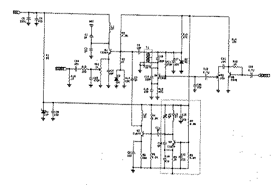
Radio transmitters for eavesdropping on private conversations and sending video pictures, battery-operated.
Radio transmitters designed for eavesdropping applications typically operate within specific frequency ranges to capture audio and video signals discreetly. These devices often utilize low-power RF (radio frequency) technology to...
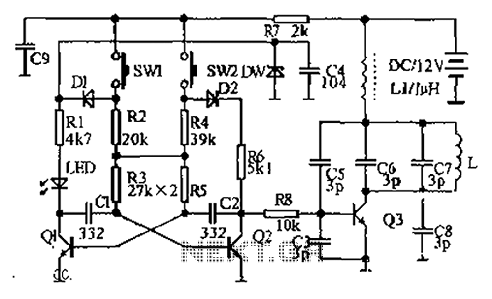
Dual AC radio remote control switch circuit diagram
The circuit diagram illustrates a dual radio remote control switch system. The transmitter section features Q3, which generates a high-frequency carrier signal, while Q1 and Q2 form the oscillator circuit. Pressing switch SW1 results in an oscillation frequency of 5...
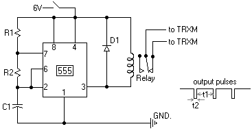
Oscillator circuit schematic
This webpage outlines the radio transmitter unit that was part of the Cirrus One rocket mission in April 2001. The transmitter was included as a payload due to concerns about recovery challenges if the rocket drifted far downrange after reaching...
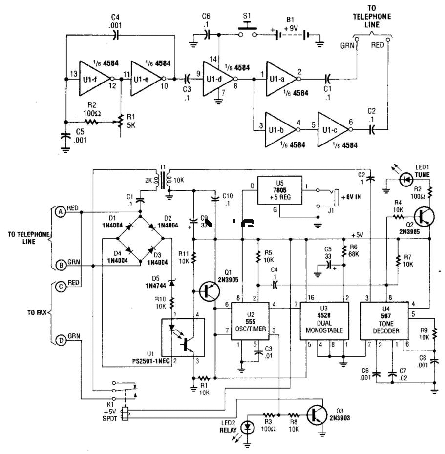
Remote-Controlled Telephone/Fax Machine Switch
This system uses a transmitter operating at approximately 100 kHz to control a remote receiver. A line splitter can connect the transmitter to the active telephone line. The transmitter is a CMOS oscillator equipped with output buffer stages to drive...
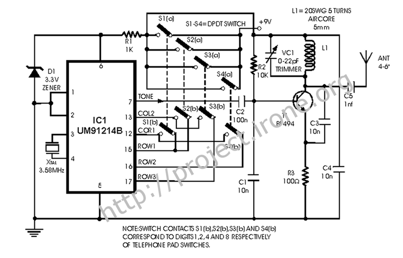
Radio frequency Of Remote Control
This is a remote control circuit that uses radio frequency electrical signals to control a variety of applications. Component: Transistor.
The remote control circuit operates by transmitting radio frequency (RF) signals to communicate with various devices. At its core, the circuit...
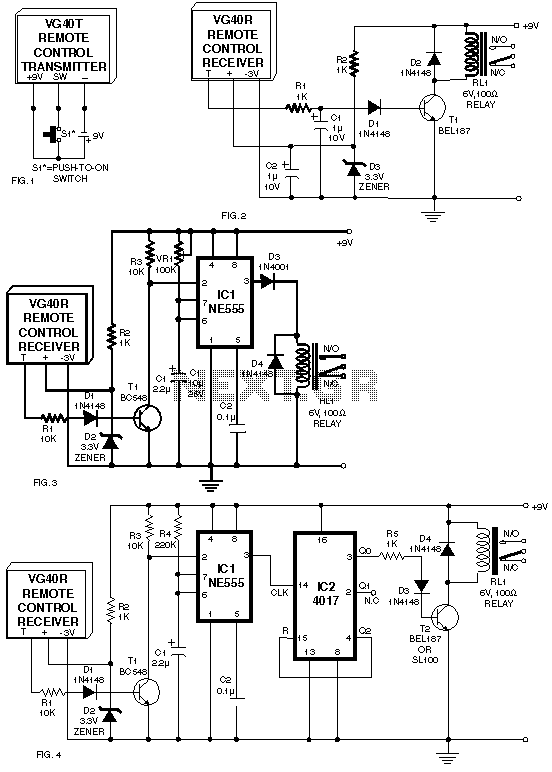
remote control for electrical
A circuit for a remote control unit utilizes radio frequency signals to operate various electrical appliances. This remote control unit features four channels, which can be expanded to twelve. Unlike typical remote control circuits that rely on infrared light for...
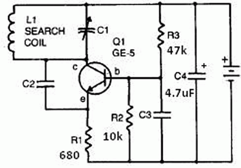
Metal detector using radio frequency
This metal detector schematic circuit is based on a transistor radio as a detector. This metal detector is entirely different from other metal detectors because this circuit does not have a speaker. With the radio tuned to a weak station,...
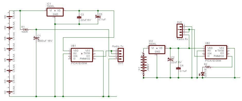
500 metre radio data link
A water tank, dam, or gate can be monitored for vehicle detection without the need for wired connections through the garden. This guide demonstrates how to transmit data reliably over a distance of 500 meters using PICAXE microcontroller chips and...
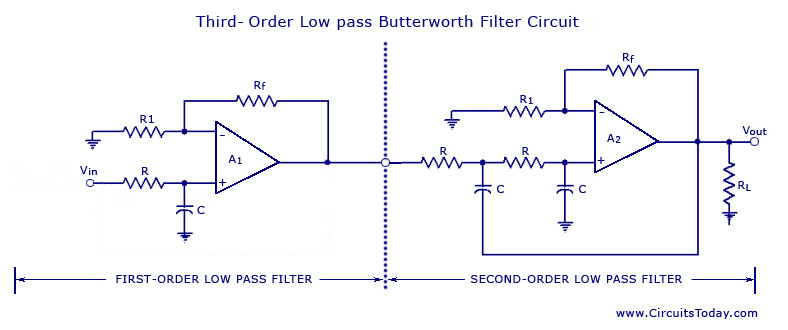
Higher Order Filters
From the discussion made so far on the filters, it can be concluded that in the stopband, the gain of the filter changes at the rate of 20 dB/decade for first-order filters and 40 dB/decade for second-order filters. This indicates...