


QPSK Demodulator Is A Good Match For Low-Cost Modulator
#QPSK
#demodulator
#modulator
#CMOS
#low-cost
#phase-shift keying
#telecommunication
#digital communication
#RF
#signal processing
Description: This demodulator is designed for the quadrature phase-shift keying (QPSK) modulator previously published by the same author in "Novel Low-Cost QPSK Modulator Needs No Adjustments" (Electronic Design, Sept. 16, 2002, p. 92). Utilizing common CMOS logic, it requires no adjustments, making it suitable for low-cost applications such as factory communications. The typical method for QPSK demodulation involves decomposing the modulated input signal using two multipliers driven by a fixed-frequency oscillator, whose outputs are 90 degrees apart. This process generates terms at twice the oscillator's frequency, necessitating the inclusion of two low-pass filters (LPFs) to eliminate these components. A parallel-to-serial converter is then employed to translate dibits into bits, resulting in the desired pulse code modulation (PCM) signal. An alternative demodulator compatible with the aforementioned QPSK modulator produces four modified carrier phases (0 degrees, 90 degrees, 180 degrees, and 270 degrees) derived from the modulator by rotating the angles of the QPSK constellation. A simple XNOR operation is performed between each phase and the modulated signal, yielding a logic "1" only if both signals coincide. If the received phase is 0 degrees (related to dibit 00), all XNORs output a logic "0." For a phase of 90 degrees (dibit 10), only the upper branch produces a "1," while the situation is inverted for 270 degrees (dibit 01), where the lower branch generates a logic "1." Conversely, for a phase of 180 degrees (dibit 11), a logic "1" is produced in both branches, resulting in the demodulated PCM signal. In practical applications, the phase-reference generator supplies inputs to the XNOR gates. Additionally, the ERROR (UART) input adjusts the initial phase reference according to the circuit described in "Automatic Phase Detector For Digital Communications" (Electronic Design, Sept. 2, 1997, p. 168). This circuit establishes a closed loop between the PCM signal and ERROR (UART), ensuring the necessary synchronization for coherent detection. Similar to the modulator, this circuit operates at a carrier frequency of fm/8 and has been tested at 2 MHz with basic CMOS logic and at 20 MHz with HCMOS.
The QPSK demodulator circuit is structured to effectively handle the modulation and demodulation of signals in a coherent manner. The primary components include two multipliers, which serve to mix the incoming modulated signal with the two quadrature outputs from the fixed-frequency oscillator. The oscillator frequency should be chosen to ensure that it is stable and accurately represents the carrier frequency of the transmitted signal. The outputs of the multipliers are then passed through low-pass filters to eliminate unwanted high-frequency components, thus allowing only the baseband signals to pass through for further processing.
The parallel-to-serial converter is crucial for transforming the dibit outputs from the multipliers into a serial bit stream, which is the format required for digital processing and transmission. The use of XNOR gates provides a straightforward mechanism to detect phase coincidences, which is essential for interpreting the dibits correctly. The design also incorporates a phase-reference generator that is critical for maintaining synchronization between the transmitted and received signals, ensuring that the demodulator can accurately process the incoming data even in the presence of phase shifts or variations in the signal.
The integration of the ERROR (UART) input allows for dynamic adjustment of the phase reference, facilitating effective phase detection and enhancing the overall reliability of the demodulation process. This feature is particularly beneficial in environments where signal conditions may fluctuate, as it enables the circuit to adaptively maintain synchronization, thereby improving communication integrity.
Overall, this demodulator design leverages cost-effective CMOS technology while providing robust performance suitable for various low-cost communication applications, particularly in industrial settings where reliable data transmission is essential.This demodulator is suitable for the quadrature phase-shift keying (QPSK) modulator previously published by the same author, "Novel Low-Cost QPSK Modulator Needs No Adjustments" (electronic design, Sept. 16, 2002, p. 92). Also based on common CMOS logic, it requires no adjustments. These characteristics make it appropriate for low-cost application s, such as factory communications. The typical approach to QPSK demodulation decomposes the modulated input signal via two multipliers driven by a fixed-frequency oscillator whose two outputs are 90 ° apart ( Fig. 1 ). This operation also produces terms at twice the rate of the oscillator. So, two low-pass filters (LPFs) are added to eliminate them. Finally, a parallel-to-serial converter translates the dibits to bits, thus producing the desired PCM signal.
An alternative demodulator that`s suitable for the aforementioned QPSK modulator generates four modified carrier phases (0 °, 90 °, 180 °, and 270 °) obtained in the modulator by rotating the angles of the QPSK constellation. Then, a simple XNOR operation between each phase and the modulated signal will produce a logic "1" only if both coincide ( Fig.
2 ). If the received phase is 0 ° (related to dibit 00), all XNORs produce a logic "0. " If the phase is 90 ° (dibit 10), only the upper branch gives a "1. " This situation is inverted for 270 ° (dibit 01). In this case, the logic "1" is produced at the lower branch. But if the phase is 180 ° (dibit 11), a logic "1" is added to both branches. The result is the demodulated PCM signal. In a practical circuit, the phase-references generator produces inputs to the XNOR gates ( Fig. 3 ). Also, the input, called ERROR (UART), adapts the initial phase reference in accordance with the circuit, "Automatic Phase Detector For Digital Communications" (electronic design, Sept. 2, 1997, p. 168). This circuit forms a closed loop between the PCM signal and ERROR (UART) that provides the necessary synchronization for coherent detection.
Like the modulator, this circuit runs for a carrier frequency of fm/8. It has been tested at 2 MHz (with basic CMOS logic) and at 20 MHz (with HCMOS).
The QPSK demodulator circuit is structured to effectively handle the modulation and demodulation of signals in a coherent manner. The primary components include two multipliers, which serve to mix the incoming modulated signal with the two quadrature outputs from the fixed-frequency oscillator. The oscillator frequency should be chosen to ensure that it is stable and accurately represents the carrier frequency of the transmitted signal. The outputs of the multipliers are then passed through low-pass filters to eliminate unwanted high-frequency components, thus allowing only the baseband signals to pass through for further processing.
The parallel-to-serial converter is crucial for transforming the dibit outputs from the multipliers into a serial bit stream, which is the format required for digital processing and transmission. The use of XNOR gates provides a straightforward mechanism to detect phase coincidences, which is essential for interpreting the dibits correctly. The design also incorporates a phase-reference generator that is critical for maintaining synchronization between the transmitted and received signals, ensuring that the demodulator can accurately process the incoming data even in the presence of phase shifts or variations in the signal.
The integration of the ERROR (UART) input allows for dynamic adjustment of the phase reference, facilitating effective phase detection and enhancing the overall reliability of the demodulation process. This feature is particularly beneficial in environments where signal conditions may fluctuate, as it enables the circuit to adaptively maintain synchronization, thereby improving communication integrity.
Overall, this demodulator design leverages cost-effective CMOS technology while providing robust performance suitable for various low-cost communication applications, particularly in industrial settings where reliable data transmission is essential.This demodulator is suitable for the quadrature phase-shift keying (QPSK) modulator previously published by the same author, "Novel Low-Cost QPSK Modulator Needs No Adjustments" (electronic design, Sept. 16, 2002, p. 92). Also based on common CMOS logic, it requires no adjustments. These characteristics make it appropriate for low-cost application s, such as factory communications. The typical approach to QPSK demodulation decomposes the modulated input signal via two multipliers driven by a fixed-frequency oscillator whose two outputs are 90 ° apart ( Fig. 1 ). This operation also produces terms at twice the rate of the oscillator. So, two low-pass filters (LPFs) are added to eliminate them. Finally, a parallel-to-serial converter translates the dibits to bits, thus producing the desired PCM signal.
An alternative demodulator that`s suitable for the aforementioned QPSK modulator generates four modified carrier phases (0 °, 90 °, 180 °, and 270 °) obtained in the modulator by rotating the angles of the QPSK constellation. Then, a simple XNOR operation between each phase and the modulated signal will produce a logic "1" only if both coincide ( Fig.
2 ). If the received phase is 0 ° (related to dibit 00), all XNORs produce a logic "0. " If the phase is 90 ° (dibit 10), only the upper branch gives a "1. " This situation is inverted for 270 ° (dibit 01). In this case, the logic "1" is produced at the lower branch. But if the phase is 180 ° (dibit 11), a logic "1" is added to both branches. The result is the demodulated PCM signal. In a practical circuit, the phase-references generator produces inputs to the XNOR gates ( Fig. 3 ). Also, the input, called ERROR (UART), adapts the initial phase reference in accordance with the circuit, "Automatic Phase Detector For Digital Communications" (electronic design, Sept. 2, 1997, p. 168). This circuit forms a closed loop between the PCM signal and ERROR (UART) that provides the necessary synchronization for coherent detection.
Like the modulator, this circuit runs for a carrier frequency of fm/8. It has been tested at 2 MHz (with basic CMOS logic) and at 20 MHz (with HCMOS).
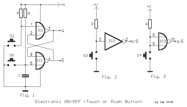
Electronic Switch ON-OFF
Here we have three choices, with which we can make electronic switches that use our touch or pressing (push button). We thus exploit the very big resistance of entry, that present the gates CMOS. In the fig.1 we have two...
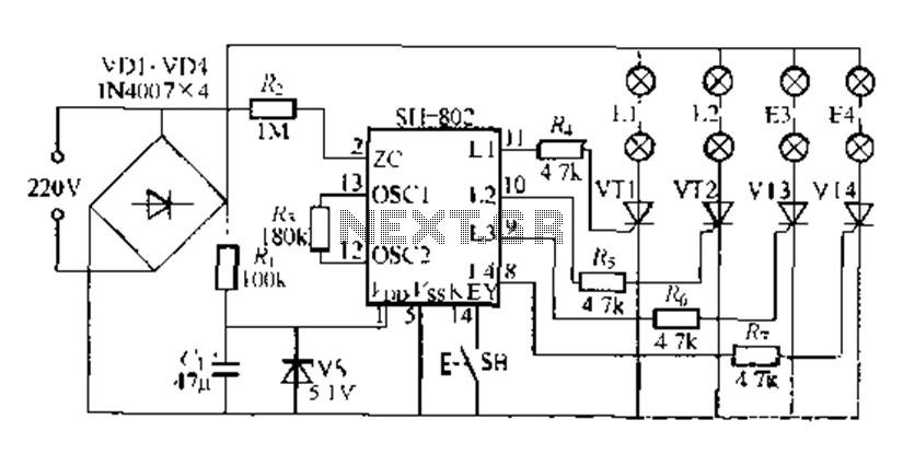
Digital integrated circuits using CMOS circuit Responder
A digital integrated circuit simplifies the response process significantly. The diagram illustrates a circuit comprising four responder groups.
The digital integrated circuit described serves as a crucial component in various electronic systems, primarily focusing on enhancing response efficiency. It comprises four...
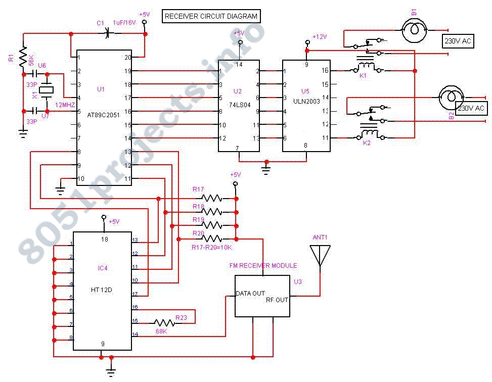
RF Remote control
The Project Long Range Remote Control can be used to remotely control a number of Electrical or Electronic Gadgets connected to it. Unlike Infra Red remote control, this Project employs FM transmission and Reception, and hence it can be used...
Bistable Multivibrators
The circuit utilizes a CMOS dual D flip-flop (CD4013) to toggle a relay or other load using a momentary push button. Multiple push buttons can be connected in parallel to control the relay from different locations. A high signal from...
CD4047 CMOS OSCILLATOR
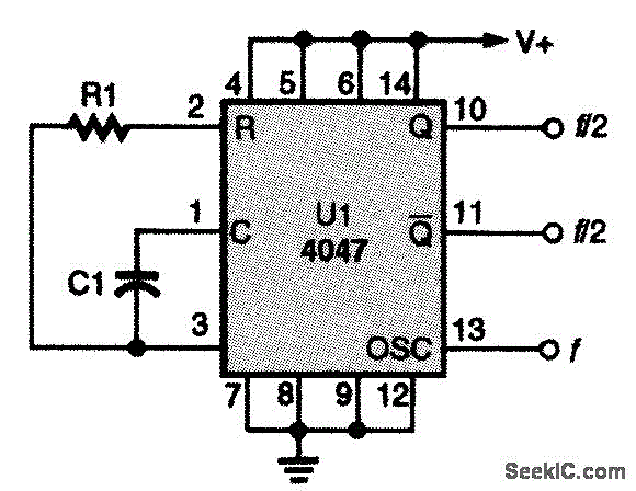
This CMOS square-wave oscillator utilizes the 4047 multivibrator circuit, suitable for both monostable (one-shot) and astable applications. In the provided configuration, the 4047 operates as an astable multivibrator. The circuit features three outputs from the 4047, with the first being...
RF Induction Meter
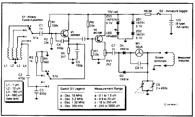
This instrument measures inductances from 0.1 microhenry to 3 millihenries, divided into four ranges set by a switch. It operates from 12 volts and is powered by eight AA type cells attached to the unit. Initially, Drew Diamond's unit in...
DOUBLE SIDEBAND SUPPRESSED CARRIER MODULATOR
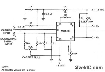
The basic current allows no carrier to be present in the output. By adding offsets to the carrier differential pairs, controlled amounts of carrier appear at the output. The amplitude becomes a function of the modulation signal—AM modulation.
In a typical...
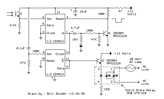
CMOS Toggle Flip Flop Using Laser Pointer circuit
The IR photo transistor Q1 (Radio Shack 276-145A) or a similar component is connected to the set input (pin 6). It is essential to shield the photo transistor from direct light to ensure that the voltage at the set input...
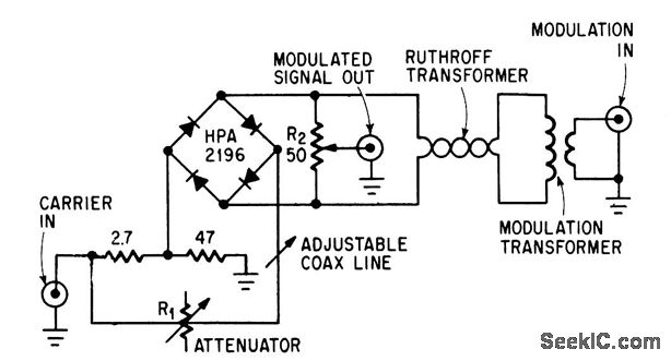
BALANCED MODULATOR DEMODULATOR
This circuit achieves high carrier and modulation suppression by utilizing closely matched diodes. It includes resistor R1 for amplitude adjustment and a coaxial line for phase adjustment. Resistor R2 allows for slight amplitude adjustments.
The described circuit is a diode...