


Time-Delay Photo-Flash Trigger
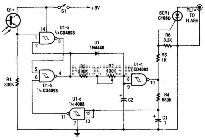
Description: Q1 is a phototransistor that is normally illuminated by a beam of light. When the beam is interrupted, pin 1 of U1A goes high, which forces pin 4 of U2B low. Consequently, capacitor C2 discharges through resistors R2 and R3. After a specified time delay, pin 10 of U1C goes high, triggering SCR1 and activating the flash. Resistor R4 and capacitor C1 charge, causing the output of U1D to go low after approximately 1 second, resetting U1A and U1B to their initial states. This delay mechanism prevents accidental double flash exposure.
The circuit utilizes a phototransistor (Q1) that serves as a light sensor, detecting the presence or absence of a light beam. When the light beam is interrupted, it signals U1A, which is likely a comparator or a logic gate, to change its output state. This transition triggers a series of events in the circuit. The low output from U2B indicates that the phototransistor has detected an interruption, leading to the discharge of capacitor C2 through resistors R2 and R3. The values of R2 and R3 will determine the discharge time constant, thereby influencing the overall delay before the next stage of the circuit is activated.
The high output from pin 10 of U1C, after the delay, activates SCR1, a silicon-controlled rectifier that is typically used for switching applications. This triggers the flash mechanism, indicating that the circuit is designed for applications such as photography or optical signaling where a flash is required upon detection of an event (e.g., interruption of a light beam).
Following the activation of the flash, the charging of capacitor C1 through resistor R4 occurs. The time constant for this charging process will be determined by the values of R4 and C1. After approximately one second, the output from U1D goes low, which serves to reset both U1A and U1B to their initial states. This reset is crucial as it ensures that the circuit can be reused without manual intervention, thereby preventing any unintended double exposure from occurring due to rapid successive light interruptions.
The design of the circuit emphasizes reliability and automation, with a built-in delay mechanism to enhance user experience by avoiding accidental triggers. The choice of components, such as the phototransistor, SCR, and timing capacitors, plays a significant role in the performance and responsiveness of the entire system. Ql is a phototransistor that is normally illuminated by a beam of light. When the beam is intercoupled, pin 1 of U1A goes high, and forces pin 4 U2B low. Then, C2 discharges through R2 and R3. After a certain time delay, pin 10 U1C goes high, triggers SCR1, and sets off the flash. R4/C1 charges, causes U1D output to go low after about 1h second, and resets U1A and U1B to the initial state. This delay prevents accidental double flash exposure.
The circuit utilizes a phototransistor (Q1) that serves as a light sensor, detecting the presence or absence of a light beam. When the light beam is interrupted, it signals U1A, which is likely a comparator or a logic gate, to change its output state. This transition triggers a series of events in the circuit. The low output from U2B indicates that the phototransistor has detected an interruption, leading to the discharge of capacitor C2 through resistors R2 and R3. The values of R2 and R3 will determine the discharge time constant, thereby influencing the overall delay before the next stage of the circuit is activated.
The high output from pin 10 of U1C, after the delay, activates SCR1, a silicon-controlled rectifier that is typically used for switching applications. This triggers the flash mechanism, indicating that the circuit is designed for applications such as photography or optical signaling where a flash is required upon detection of an event (e.g., interruption of a light beam).
Following the activation of the flash, the charging of capacitor C1 through resistor R4 occurs. The time constant for this charging process will be determined by the values of R4 and C1. After approximately one second, the output from U1D goes low, which serves to reset both U1A and U1B to their initial states. This reset is crucial as it ensures that the circuit can be reused without manual intervention, thereby preventing any unintended double exposure from occurring due to rapid successive light interruptions.
The design of the circuit emphasizes reliability and automation, with a built-in delay mechanism to enhance user experience by avoiding accidental triggers. The choice of components, such as the phototransistor, SCR, and timing capacitors, plays a significant role in the performance and responsiveness of the entire system. Ql is a phototransistor that is normally illuminated by a beam of light. When the beam is intercoupled, pin 1 of U1A goes high, and forces pin 4 U2B low. Then, C2 discharges through R2 and R3. After a certain time delay, pin 10 U1C goes high, triggers SCR1, and sets off the flash. R4/C1 charges, causes U1D output to go low after about 1h second, and resets U1A and U1B to the initial state. This delay prevents accidental double flash exposure.
Automatic Room light Control With Bi Directional Visitor Counter
The objective of this project is to create a controller-based model that counts the number of individuals entering a specific room and activates the lighting accordingly. This is achieved through the use of sensors that detect the current number of...
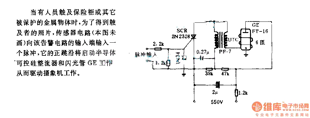
The alarm circuit diagram for safety box and other metal objects
When an individual touches the safety box or other protected metal objects, the sensor circuit generates a pulse to the alarm circuit. The positive edge of this pulse activates the semiconductor and thyristor flash GE, subsequently triggering the camera to...
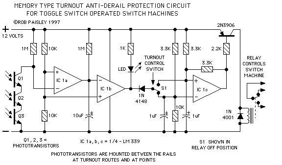
Protector
The circuits presented here will prevent turnouts from being thrown while a train is on a switch, which is ideal in situations where the switch cannot be seen by the operator. They utilize phototransistor sensors to detect the presence of...
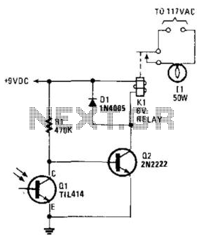
Simple Photoelectric Light Controller
A phototransistor detects daylight. At dusk, it stops conducting, and Rl biases Q2, activating Kl, which turns on the light. At dawn, Ql begins to conduct, cutting off Q2. Kl deactivates, and the light turns off.
The circuit utilizes a phototransistor...
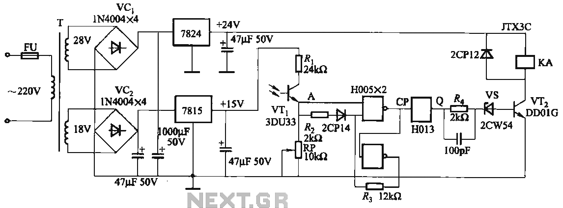
Photoelectric controller circuit immunity
The circuit features a robust anti-jamming capability, making it suitable for demanding applications. It includes a phototransistor (VTi), a Schmitt trigger (H005), a JK flip-flop (H013), a power amplifier circuit, a relay (KA), and various actuators and other components. The...
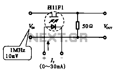
Optical attenuation control circuit
A phototransistor, also referred to as a photosensitive transistor, is primarily utilized as a photosensitive device. It is characterized by its ability to adjust impedance in relation to the intensity of incoming light, similar to that of photosensitive resistors and...
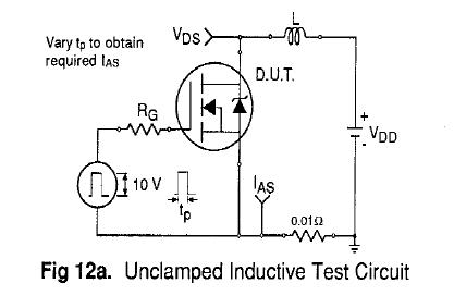
circuits
Uploaded with ImageShack.us Uploaded with ImageShack.us Uploaded with ImageShack.us Inquiry regarding experiences with specific circuits.
In this context, the inquiry pertains to the performance and functionality of certain electronic circuits that have been shared via an image hosting service. The request...
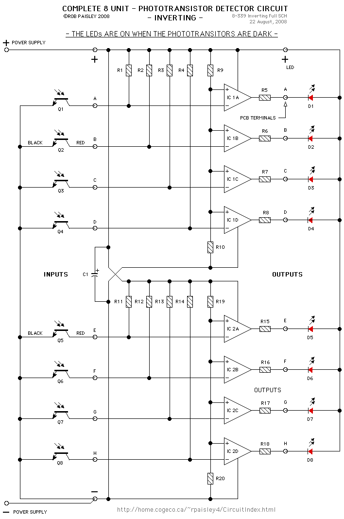
Photo Inverting
For phototransistors, a resistance value of 470K ohms is suitable for most ambient light conditions. In cases of dim lighting, a higher resistor value, such as 1 Megohm, can enhance sensitivity. This high-impedance test voltmeter circuit is also applicable for...
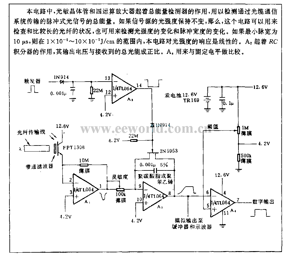
Optical transmission detection circuit
This circuit employs a phototransistor along with four operational amplifiers to function as a total energy detector. It is designed to measure the total energy of optical pulses transmitted through an optical cable communication system. When the light intensity of...