


A part of product detector circuit composed of LF198 and LM122H
#LF198
#LM122H
#timer circuit
#synchronous clock
#pulse width
#sampling
#holding control
#noise
#signal processing
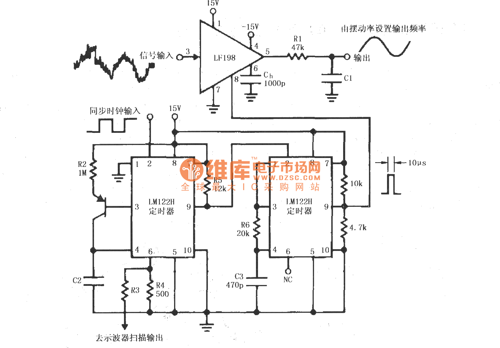
Description: A synchronous clock signal is fed into a cascade of timer circuits composed of two LM122H devices. The synchronization clock is then converted into a pulse of the desired width, which is added to the LF198 logic end (pin 8) as the sampling and holding control signal. This signal is input to pin 3 of the LF198. The input signal contains a significant amount of noise.
The circuit operates by utilizing two LM122H timer ICs configured in a cascading arrangement. The first LM122H receives the synchronous clock signal and generates a pulse that is subsequently modified by the second LM122H. This configuration allows for precise control over the pulse width, which is critical for applications requiring accurate timing and synchronization.
The LF198 is a sample-and-hold amplifier that is designed to capture and hold the voltage of an input signal for a specified duration. In this setup, the output pulse from the LM122H timers serves as the control signal for the LF198, dictating when the device samples the input signal. The control signal is connected to pin 8 of the LF198, enabling the device to operate effectively in a sampling mode.
It is important to note that the input signal presented to the LF198 at pin 3 may contain various noise components. This noise can adversely affect the performance of the sample-and-hold circuit, potentially leading to inaccurate voltage readings. Therefore, appropriate filtering techniques may be required to clean the input signal before it reaches the LF198. Implementing low-pass filters or other noise-reduction strategies can help ensure that the sampled signal is as clean as possible, thus improving the overall performance of the circuit.
In summary, the described circuit effectively utilizes LM122H timer ICs to generate a controlled pulse width from a synchronous clock signal, which is then used to control the sampling process of the LF198. Careful consideration of noise management is essential for optimal circuit functionality.Synchronous clock signal is input to a cascade of timer circuit composed of two LM122H, then the synchronization clock is converted to the desired width of the pulse (Fig. 10?s) which will be add to LF198 LOGIC end (8 feet) as the sampling and holding control signal. The signal is input LF198`s pin 3. The input signal contains a large number of noise com..
The circuit operates by utilizing two LM122H timer ICs configured in a cascading arrangement. The first LM122H receives the synchronous clock signal and generates a pulse that is subsequently modified by the second LM122H. This configuration allows for precise control over the pulse width, which is critical for applications requiring accurate timing and synchronization.
The LF198 is a sample-and-hold amplifier that is designed to capture and hold the voltage of an input signal for a specified duration. In this setup, the output pulse from the LM122H timers serves as the control signal for the LF198, dictating when the device samples the input signal. The control signal is connected to pin 8 of the LF198, enabling the device to operate effectively in a sampling mode.
It is important to note that the input signal presented to the LF198 at pin 3 may contain various noise components. This noise can adversely affect the performance of the sample-and-hold circuit, potentially leading to inaccurate voltage readings. Therefore, appropriate filtering techniques may be required to clean the input signal before it reaches the LF198. Implementing low-pass filters or other noise-reduction strategies can help ensure that the sampled signal is as clean as possible, thus improving the overall performance of the circuit.
In summary, the described circuit effectively utilizes LM122H timer ICs to generate a controlled pulse width from a synchronous clock signal, which is then used to control the sampling process of the LF198. Careful consideration of noise management is essential for optimal circuit functionality.Synchronous clock signal is input to a cascade of timer circuit composed of two LM122H, then the synchronization clock is converted to the desired width of the pulse (Fig. 10?s) which will be add to LF198 LOGIC end (8 feet) as the sampling and holding control signal. The signal is input LF198`s pin 3. The input signal contains a large number of noise com..
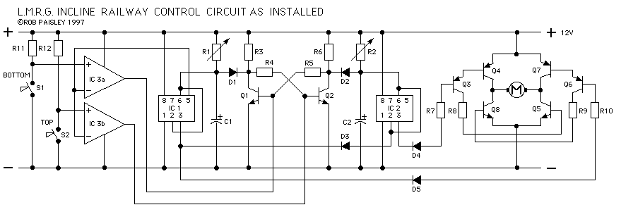
Incline Railway Project
The drawings and photos below are for an operating incline railway that was built by the London Model Railroad Group for its O scale model railway club located at London, Ontario, Canada. This is a single car model loosely based...
Incline Railway Project
The drawings and photos below are for an operating incline railway that was built by the London Model Railroad Group for its O scale model railway club located at London, Ontario, Canada. This is a single car model loosely based...
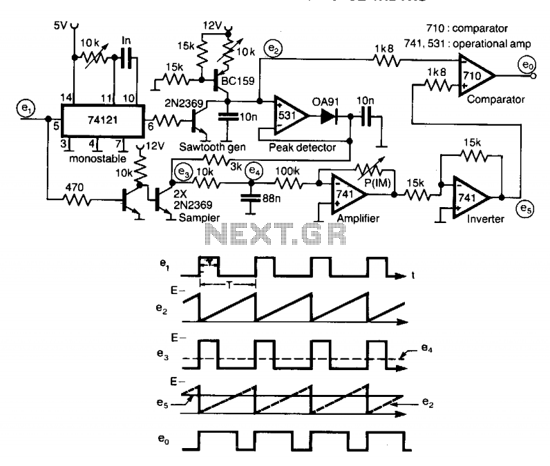
Multiplying pulse widths circuit
A circuit designed to multiply the width of incoming pulses by a factor that can be greater or less than unity is straightforward to construct. It features a single adjustable potentiometer for selecting the multiplying factor. This factor is established...
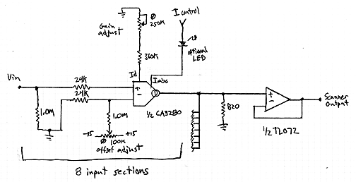
Interpolating Scanner Circuit
This design is for an interpolating scanner, a circuit featuring multiple signal inputs, a control voltage input, and a signal output. The output selectively transitions between inputs, smoothly fading from one to the next as the control voltage increases. A...
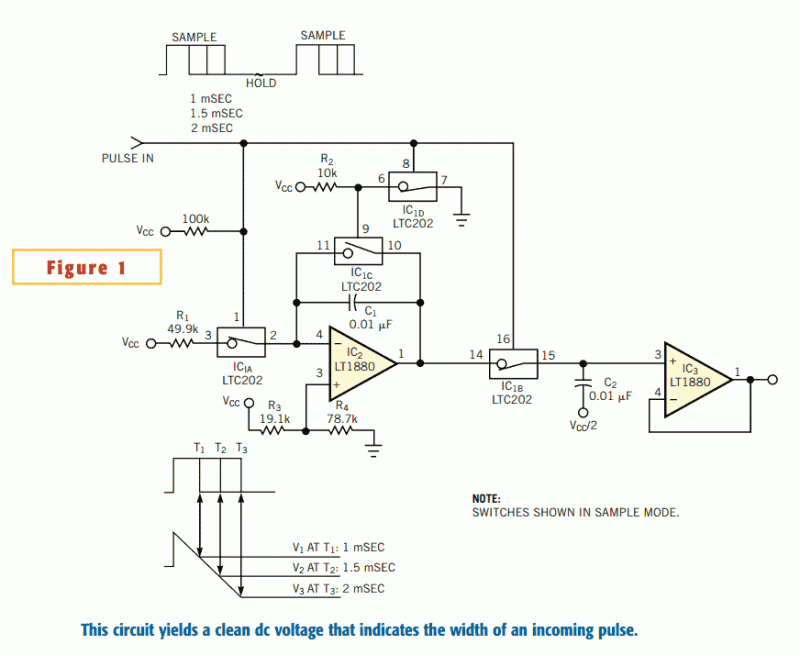
Circuit converts pulse width to voltage
The circuit in Figure 1 converts pulse information to a clean dc voltage by the end of a single incoming pulse. In another technique, an RC filter can convert a PWM signal to an averaged dc voltage, but this method...