


Pulse-height-to-width-converter
#pulse conversion
#linear function
#input threshold
#zener diode
#transistor
#pulse width
#pulse height
#circuit discrimination
#pulse repetition rate
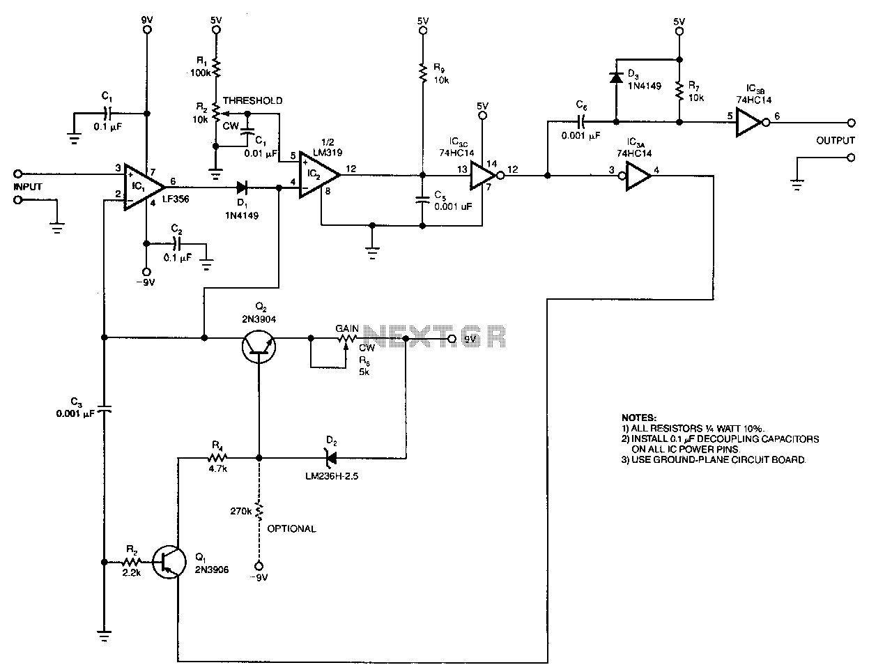
Description: The output pulse width from the circuit is a linear function of the input pulse height. The circuit's input threshold can be set to discriminate against low-level pulses, while fixed components limit the maximum output pulse width. With a 270 kΩ resistor connected from the -9 V supply to the base lead of Q2, this circuit can handle input pulses separated by 20 µs for correct operation. The turn-off time of zener diode D2 sets the lower limit for the input pulse repetition rate. IC1, D1, and C3 detect the peak of the input pulse. The comparator IC2 triggers at a preset threshold. The RC delay network, consisting of R9 and C5, holds off inverter IC3's changing state until peak detection is complete. After IC3A changes state, Q1 turns on and subsequently activates Q2, a constant-current source. Constant-current source Q1 then discharges C3, the peak-detecting capacitor. When C3 discharges below IC2's threshold, IC2's output decreases, as do pins 6 and 4 of IC3. The output pulse width is a function of this discharge time, which can be adjusted with R6. C6 and R7 control the maximum output pulse width, which is 8 µs maximum.
The described circuit operates as a pulse width modulation (PWM) generator, where the output pulse width is directly proportional to the height of the input pulse. The adjustable input threshold allows for flexibility in distinguishing between valid input signals and noise, thereby enhancing the circuit's reliability in various applications. The use of a 270 kΩ resistor connected to the -9 V supply ensures that the circuit can effectively handle rapid input pulse sequences with a minimum separation of 20 µs, making it suitable for high-speed applications.
The peak detection mechanism is facilitated by the components IC1, D1, and C3, which work together to capture the maximum voltage level of the incoming pulse. The comparator IC2 is crucial in this design, as it provides a trigger point that is adjustable based on the application requirements. The RC delay network formed by R9 and C5 introduces a delay that prevents premature switching of the inverter IC3 until the peak detection process is fully completed. This design choice minimizes the risk of erroneous output due to rapid fluctuations in the input signal.
Once the peak detection is confirmed, the inverter IC3A transitions state, which activates the constant-current source Q1. This source is responsible for discharging the peak-detecting capacitor C3. The discharge time of C3 is critical, as it determines the output pulse width. The adjustment of R6 allows for fine-tuning of this discharge time, providing additional flexibility in output characteristics.
Moreover, the maximum output pulse width is regulated by components C6 and R7, ensuring that the output does not exceed 8 µs. This feature is particularly important in applications where precise control over pulse timing is essential. Overall, this circuit design showcases an efficient method for generating output pulses that are dependent on input signal characteristics while incorporating safeguards against undesired low-level signals.The output-pulse width from the circuit is a linear function of the input pulse"s height. You can set the circuit"s input threshold to discriminate against low-level pulses, while fixed components limit the circuit"s maximum output -pulse width. With a 270-KO resistor connected from the -9 V supply to the base lead of Q2, this circuit can handle input pulses separated by 20 p.s for correct operation.
The tum-off time of zener diode D2 sets the lower limit for the input-pulse repetition rate. IC1, D1, and C3 detect the peak of the input pulse. The comparator IC2, triggers at your preset threshold. The RC del
Related Circuits
The described circuit operates as a pulse width modulation (PWM) generator, where the output pulse width is directly proportional to the height of the input pulse. The adjustable input threshold allows for flexibility in distinguishing between valid input signals and noise, thereby enhancing the circuit's reliability in various applications. The use of a 270 kΩ resistor connected to the -9 V supply ensures that the circuit can effectively handle rapid input pulse sequences with a minimum separation of 20 µs, making it suitable for high-speed applications.
The peak detection mechanism is facilitated by the components IC1, D1, and C3, which work together to capture the maximum voltage level of the incoming pulse. The comparator IC2 is crucial in this design, as it provides a trigger point that is adjustable based on the application requirements. The RC delay network formed by R9 and C5 introduces a delay that prevents premature switching of the inverter IC3 until the peak detection process is fully completed. This design choice minimizes the risk of erroneous output due to rapid fluctuations in the input signal.
Once the peak detection is confirmed, the inverter IC3A transitions state, which activates the constant-current source Q1. This source is responsible for discharging the peak-detecting capacitor C3. The discharge time of C3 is critical, as it determines the output pulse width. The adjustment of R6 allows for fine-tuning of this discharge time, providing additional flexibility in output characteristics.
Moreover, the maximum output pulse width is regulated by components C6 and R7, ensuring that the output does not exceed 8 µs. This feature is particularly important in applications where precise control over pulse timing is essential. Overall, this circuit design showcases an efficient method for generating output pulses that are dependent on input signal characteristics while incorporating safeguards against undesired low-level signals.The output-pulse width from the circuit is a linear function of the input pulse"s height. You can set the circuit"s input threshold to discriminate against low-level pulses, while fixed components limit the circuit"s maximum output -pulse width. With a 270-KO resistor connected from the -9 V supply to the base lead of Q2, this circuit can handle input pulses separated by 20 p.s for correct operation.
The tum-off time of zener diode D2 sets the lower limit for the input-pulse repetition rate. IC1, D1, and C3 detect the peak of the input pulse. The comparator IC2, triggers at your preset threshold. The RC del
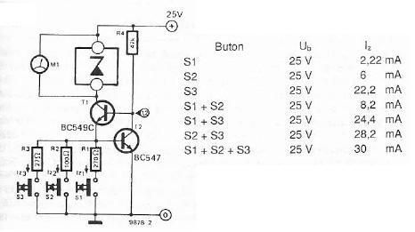
zener diode tester schematic
The electronic scheme provided can be used to design a Zener diode tester utilizing a few electronic components. This Zener tester, in conjunction with a multimeter, allows for the precise measurement of the threshold voltage of a Zener diode. The...
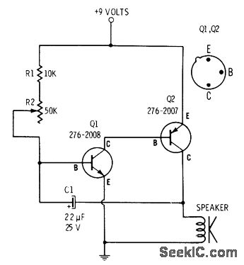
transistors How does this circuit diagram work
R2 controls the charging speed of capacitor C1. At a specific charge level, C1 triggers transistors Q1 and Q2, which release a 9-volt pulse. This pulse generates a clicking sound. The discharge process of the capacitor involves it charging gradually...
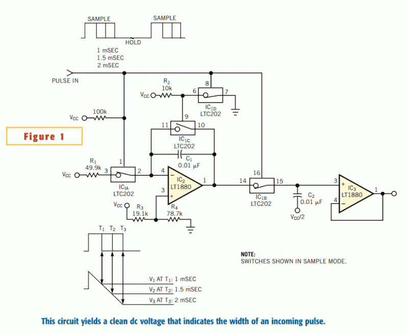
Circuit converts pulse width to voltage
The circuit in Figure 1 converts pulse information to a clean dc voltage by the end of a single incoming pulse. In another technique, an RC filter can convert a PWM signal to an averaged dc voltage, but this method...
Transistor Circuit Analysis
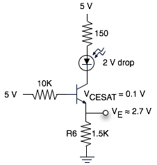
The schematic represents a relatively simple transistor circuit. Analyzing such schematics evokes memories of college days spent studying electrical engineering. However, the complexity of the schematic can be daunting after a long time away from the subject. To refresh knowledge,...
Zener Oscillator circuits
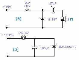
These two circuits are interesting from an academic point of view. Their practical implementation is rather critical and it is not easy to get steady operation. Circuit (a) requires a "cooked" zener: connect it first to a constant current generator,...
Simple Transistor Amplifier Circuit Schematic and Explanation
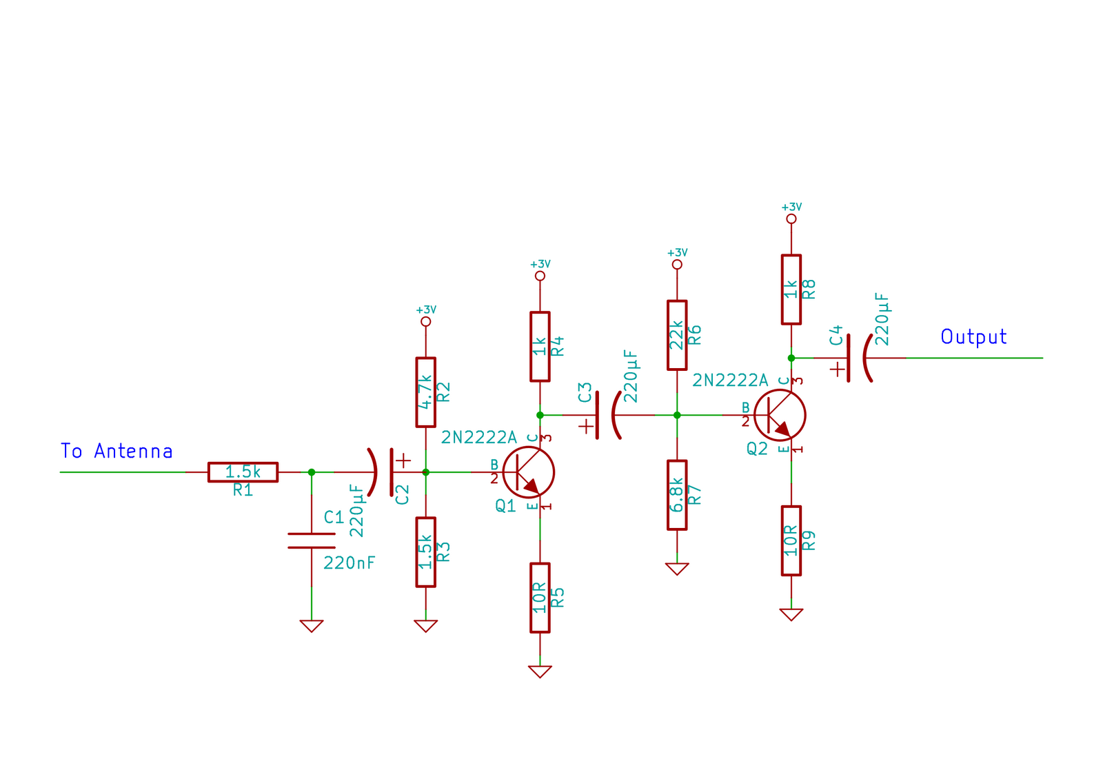
This circuit does not function as effectively as it could. It was created when the designer had a limited understanding of circuit design. An improved schematic will be developed and posted later, featuring a better design. The schematic indicates "antenna,"...

Kapanadze 5
The emitter voltage drops completely to 0V from 42V during the pulse when the transistor is conducting or saturated. This contrasts with a pure resistive load (the 4.7 Ohm resistor mentioned in the previous video), where the collector-emitter voltage does...
TUNED-COLLECTOR ARMSTRONG OSCILLATOR
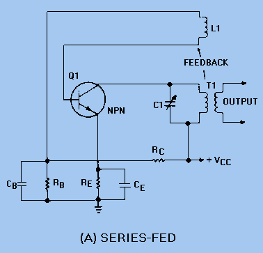
The DC path is established from the negative side (ground) of VCC through RE, Q1, T1, and returns to the positive side of VCC. The figure clearly illustrates that both the AC and DC components flow through the tank circuit....
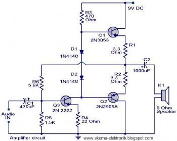
simple audio amplifier
The initial section of the circuit is a preamplifier that utilizes transistor Q1 (2N2222). The collector of transistor Q3 is connected to the base of transistor Q2 (2N2905A), which creates a complementary symmetry pair with Q3 (2N3053). The amplified signal...