


bjt transistor circuit finding the resistances
#BJT
#resistance calculation
#Q-point
#transistor biasing
#circuit analysis
#VCE
#VBE
#IC
#beta
#current gain
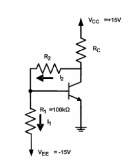
Description: A circuit diagram has been provided for analysis, with the objective of calculating the values of resistors R2 and RC. The circuit is designed to operate at the Q-point with the following parameters: VCE = 5V, VBE = 0.7V, IC = 2mA, and β = 100 (where β = IC/IB). The collector current is established at 2 mA, and VCE is measured at 5V. Given that the emitter is grounded, the collector voltage is also 5V, indicating that the voltage across RC is 10V, which is the difference between 5V and 15V. Consequently, RC can be calculated as 10V / 0.002A = 5kΩ.
For resistors R1 and R2, which create a voltage divider spanning from -15V to +5V, it is necessary to configure them such that the top of R1 reaches 0.7V (VBE). The voltage divider thus spans a total of 20V, with the 0.7V base voltage being 15.7V above the lower end of the voltage divider. It is important to note that the base current can be considered negligible in many transistor circuit analyses; however, due to the high resistance of R1, this assumption may not hold. The base current, calculated as 2mA divided by β, amounts to 0.02mA or 20µA. To find the current flowing through R1, one must consider its resistance and the voltage of 15.7V across it. The current through R2 is the total of the base current (0.02mA) and the current through R1. With the current through R2 and the voltage across it known, the resistance of R2 can be determined.
The circuit analysis begins with the identification of the required parameters for the transistors in use. The collector current (IC) is set at 2mA, which indicates the operational state of the transistor. The collector-emitter voltage (VCE) is specified as 5V, which is critical for determining the voltage drop across the collector resistor (RC). The calculation of RC is straightforward: with a voltage drop of 10V across it (the difference between the supply voltage and VCE), the resistance can be derived using Ohm’s law.
Next, the voltage divider formed by R1 and R2 must be correctly configured to ensure the base of the transistor is biased at 0.7V. The voltage divider's total voltage range is 20V, spanning from -15V to +5V. The voltage at the top of R1, which should be at 0.7V, indicates that the voltage divider must be appropriately designed to achieve this biasing condition.
Given that R1 has a high resistance value, the base current (IB) cannot be neglected in this analysis. The base current, which is a function of the collector current and the transistor's current gain (β), is calculated as 20µA. This current flows through R1, and the total current through R2 will be the sum of the base current and the current flowing through R1.
To finalize the calculations, the current through R1 needs to be determined based on its resistance and the voltage across it. Subsequently, the total current through R2 can be calculated, allowing for the determination of R2's resistance using Ohm's law, as the voltage across R2 is known. This comprehensive analysis ensures that both resistors are accurately calculated for the desired operation of the transistor circuit.I have been given the following circuit diagram and have been asked to compute R2 and RC such that, at the Q-point, the circuit will behave as follows: VCE=5V VBE=0.7V IC=2mA β=100(where β=ic/ib) There are many places we can begin looking at this. We know that the collector current is 2 mA, and that VCE is 5V. Since the emitter is at ground, the collector must be at 5V, and so the voltage across RC is therefore 10V: the difference between 5V and 15V. So RC must be 10V/.002A=5KΩ. Next, R2 and R1 which span a voltage from −15V to +5V must form a voltage divider such that the top of R1 is at 0.7V (VBE).
Hint: the voltage divider spans a range of 20V, and the 0.7V transistor base voltage is 15.7V above the bottom of the voltage divider. This approach assumes that we can ignore the base current because it is small. Often when analyzing transistor circuits we can do that, but not in this case because R1 is such a high resistor.
The voltage divider is not "stiff" at all with regard to the resistance in the base circuit of the transistor (which has no emitter resistor at all). A more exact answer requires that we account for the base current. The transistor is carrying only 2mA of current, and so is nowhere near hard saturation, and so the base current is only 0.02 mA, or 20 micro-Amperes (2mA divided by β).
Determine how much current is flowing through R1 from its resistance, and 15.7 voltage. The current flowing through R2 is the sum of the transistor base current (.02 mA) and the current through R1. Knowing the current through R2 and the voltage across it, we can calculate its resistance.
For resistors R1 and R2, which create a voltage divider spanning from -15V to +5V, it is necessary to configure them such that the top of R1 reaches 0.7V (VBE). The voltage divider thus spans a total of 20V, with the 0.7V base voltage being 15.7V above the lower end of the voltage divider. It is important to note that the base current can be considered negligible in many transistor circuit analyses; however, due to the high resistance of R1, this assumption may not hold. The base current, calculated as 2mA divided by β, amounts to 0.02mA or 20µA. To find the current flowing through R1, one must consider its resistance and the voltage of 15.7V across it. The current through R2 is the total of the base current (0.02mA) and the current through R1. With the current through R2 and the voltage across it known, the resistance of R2 can be determined.
The circuit analysis begins with the identification of the required parameters for the transistors in use. The collector current (IC) is set at 2mA, which indicates the operational state of the transistor. The collector-emitter voltage (VCE) is specified as 5V, which is critical for determining the voltage drop across the collector resistor (RC). The calculation of RC is straightforward: with a voltage drop of 10V across it (the difference between the supply voltage and VCE), the resistance can be derived using Ohm’s law.
Next, the voltage divider formed by R1 and R2 must be correctly configured to ensure the base of the transistor is biased at 0.7V. The voltage divider's total voltage range is 20V, spanning from -15V to +5V. The voltage at the top of R1, which should be at 0.7V, indicates that the voltage divider must be appropriately designed to achieve this biasing condition.
Given that R1 has a high resistance value, the base current (IB) cannot be neglected in this analysis. The base current, which is a function of the collector current and the transistor's current gain (β), is calculated as 20µA. This current flows through R1, and the total current through R2 will be the sum of the base current and the current flowing through R1.
To finalize the calculations, the current through R1 needs to be determined based on its resistance and the voltage across it. Subsequently, the total current through R2 can be calculated, allowing for the determination of R2's resistance using Ohm's law, as the voltage across R2 is known. This comprehensive analysis ensures that both resistors are accurately calculated for the desired operation of the transistor circuit.I have been given the following circuit diagram and have been asked to compute R2 and RC such that, at the Q-point, the circuit will behave as follows: VCE=5V VBE=0.7V IC=2mA β=100(where β=ic/ib) There are many places we can begin looking at this. We know that the collector current is 2 mA, and that VCE is 5V. Since the emitter is at ground, the collector must be at 5V, and so the voltage across RC is therefore 10V: the difference between 5V and 15V. So RC must be 10V/.002A=5KΩ. Next, R2 and R1 which span a voltage from −15V to +5V must form a voltage divider such that the top of R1 is at 0.7V (VBE).
Hint: the voltage divider spans a range of 20V, and the 0.7V transistor base voltage is 15.7V above the bottom of the voltage divider. This approach assumes that we can ignore the base current because it is small. Often when analyzing transistor circuits we can do that, but not in this case because R1 is such a high resistor.
The voltage divider is not "stiff" at all with regard to the resistance in the base circuit of the transistor (which has no emitter resistor at all). A more exact answer requires that we account for the base current. The transistor is carrying only 2mA of current, and so is nowhere near hard saturation, and so the base current is only 0.02 mA, or 20 micro-Amperes (2mA divided by β).
Determine how much current is flowing through R1 from its resistance, and 15.7 voltage. The current flowing through R2 is the sum of the transistor base current (.02 mA) and the current through R1. Knowing the current through R2 and the voltage across it, we can calculate its resistance.
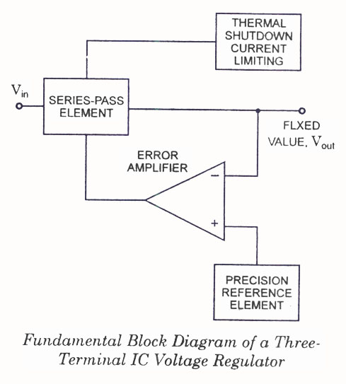
IC Voltage Regulators-withCircuit - Design & Theory
IC Voltage Regulators - Circuit diagram and block diagram of linear, fixed, adjustable (positive and negative), and switching voltage regulators.
IC voltage regulators are essential components in electronic circuits, providing stable output voltages from a varying input voltage source. They can...
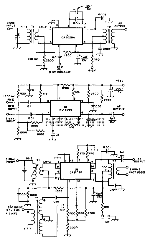
Ic Product Detectors
These product detectors utilize integrated circuit (IC) devices. They are capable of detecting single sideband (SSB) and continuous wave (CW) signals. The circuits are designed to operate effectively up to frequencies of 20 or 30 MHz. T3 in the schematic...
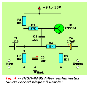
Practical Transistor Circuits
The final article on bipolar junction transistors (BJT) presents a variety of circuits, some practical and others more experimental. These circuits are capable of amplifying signals, filtering high and low frequencies, generating white noise, and flashing lamps. They can also...
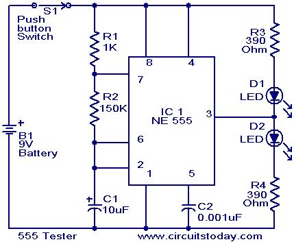
Understanding Circuit Schematics
This schematic requires clarification. It is assumed that pin 2 is connected by a wire to pin 6, although this connection appears to be unclear.
The circuit in question involves a schematic where pin 2 and pin 6 are interconnected. To...
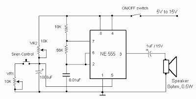
Factory Alarm
The frequency is controlled by pin 5 of the integrated circuit (IC). When the power supply is activated, the capacitor charges gradually, which alters the voltage at pin 5 of the IC, causing the frequency to increase incrementally. Once the...

The low-powered BJT base pin cast differentiates the circuit cipher scheme automatically
In electronic technology, the triode utilizes a variety of general components and parts. The parameters of the triode and numerous electrical parametric measurement schemes are closely related to measurement results. Therefore, in electronic design, the base pin, typological judgment, and...
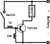
BJT H-bridge Implementation
The circuit employs a complementary pair of transistors, resulting in a symmetrical design for the H-bridge configuration. The upper corners of the H-bridge are referred to as "sources," indicating their role in supplying current to the load, which in this...
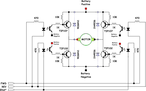
BJT H-bridge Circuit Details
The opto-isolator LEDs are connected to three wires labeled "FWD," "REV," and "ENA." These wires serve as the interface between the bridge and the microprocessor. It is important to note that there is no "ground" signal present. When connecting these...

PC-ECAP
Analyze your circuits before you build them!
PC-ECAP has been one of the world's best linear circuit analysis programs. The software will calculate and plot: gain, phase, group delay, impedance, VSWR, and return loss. This versatile program can also calculate your...