


7805 Turn-On Circuit Circuit
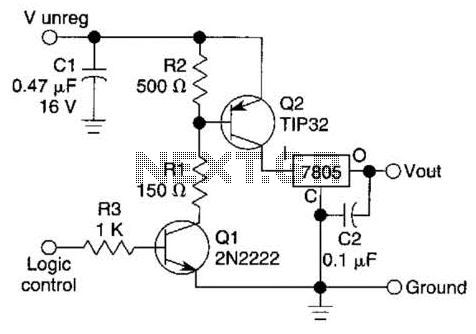
Description: A logic level can control a 7805 regulator with this circuit. Q2 is a series switching transistor controlled by Q1. Q1 is turned on by a logic voltage to its base.
This circuit utilizes a 7805 voltage regulator, which is designed to output a stable 5V supply from a higher input voltage. The control mechanism is implemented via two transistors, Q1 and Q2. Q1 functions as a control switch that is activated by a logic-level voltage applied to its base. When this voltage is present, Q1 enters the saturation region, allowing current to flow from its collector to its emitter. This action effectively turns on Q2, which is configured as a series switching transistor.
Q2, when activated by Q1, connects the output of the 7805 regulator to the load. This configuration enables the circuit to control the power delivery to the load based on the logic-level signal applied to Q1. The 7805 regulator maintains a constant 5V output as long as the input voltage remains within the specified range and the load does not exceed its current rating.
In practical applications, this circuit can be used in microcontroller-based systems where a digital output pin can control the power to various peripherals or components. The use of transistors allows for efficient switching, minimizing power loss and heat generation compared to mechanical relays. Proper biasing of the transistors is essential to ensure reliable operation, and appropriate resistor values should be selected to limit the base current for Q1 while ensuring that Q2 can handle the load current without entering the saturation region excessively.
Additionally, it is advisable to include bypass capacitors near the input and output of the 7805 to stabilize the voltage and filter out noise, ensuring clean power delivery to the connected load. A logic level can control a 7805 regulator with this circuit. Q2 is a series switcliing transistor controlled by Ql. Ql is turned on by a logic voltage to its base.
This circuit utilizes a 7805 voltage regulator, which is designed to output a stable 5V supply from a higher input voltage. The control mechanism is implemented via two transistors, Q1 and Q2. Q1 functions as a control switch that is activated by a logic-level voltage applied to its base. When this voltage is present, Q1 enters the saturation region, allowing current to flow from its collector to its emitter. This action effectively turns on Q2, which is configured as a series switching transistor.
Q2, when activated by Q1, connects the output of the 7805 regulator to the load. This configuration enables the circuit to control the power delivery to the load based on the logic-level signal applied to Q1. The 7805 regulator maintains a constant 5V output as long as the input voltage remains within the specified range and the load does not exceed its current rating.
In practical applications, this circuit can be used in microcontroller-based systems where a digital output pin can control the power to various peripherals or components. The use of transistors allows for efficient switching, minimizing power loss and heat generation compared to mechanical relays. Proper biasing of the transistors is essential to ensure reliable operation, and appropriate resistor values should be selected to limit the base current for Q1 while ensuring that Q2 can handle the load current without entering the saturation region excessively.
Additionally, it is advisable to include bypass capacitors near the input and output of the 7805 to stabilize the voltage and filter out noise, ensuring clean power delivery to the connected load. A logic level can control a 7805 regulator with this circuit. Q2 is a series switcliing transistor controlled by Ql. Ql is turned on by a logic voltage to its base.
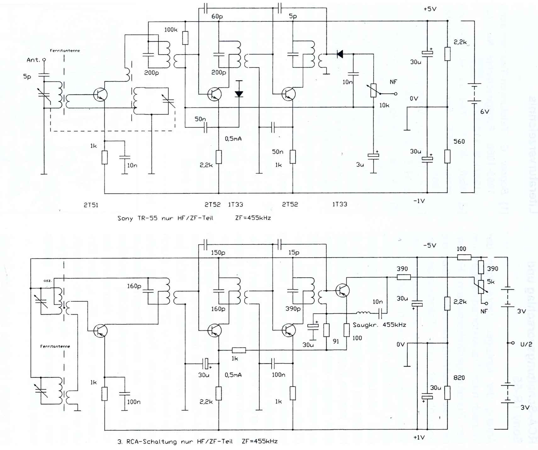
Comments on the Circuits of the first Transistor Radios
The circuitry of the Regency exhibits several unique characteristics. Notable features include the self-oscillating mixer stage, the base bias voltage of the second IF stage derived from the AF power stage, an unusual IF frequency of 262 kHz, and a...
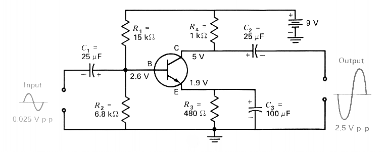
TYPICAL TRANSISTOR CIRCUIT
This is a silicon transistor circuit showing typical voltage values. When the forward base/emitter voltage is 0.6 to 0.7 V, the transistor is silicon. Germanium transistors will have a forward base/emitter bias voltage of 0.2 to 0.3 V. This is...
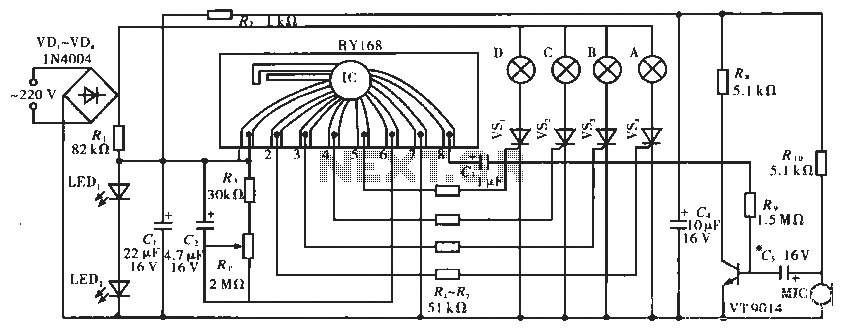
Lighting controller circuit
The circuit operates with a controller that includes a power supply circuit, a control circuit, and an audio amplifier, which are three distinct components. The power circuit comprises diodes VD1 to VD4, resistor R1, capacitor C1, LED1, LED2, and additional...
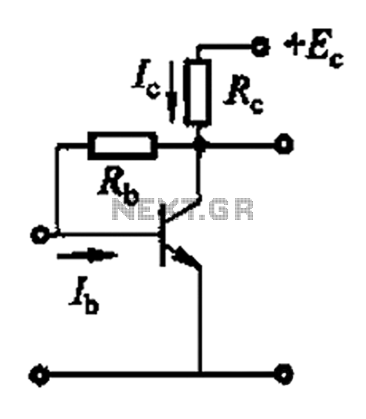
Basic reference bias circuit transistor - negative voltage feedback
Basic reference bias circuit using a transistor with negative voltage feedback.
The basic reference bias circuit utilizing a transistor with negative voltage feedback is designed to provide a stable output voltage or current that is largely independent of variations in temperature...
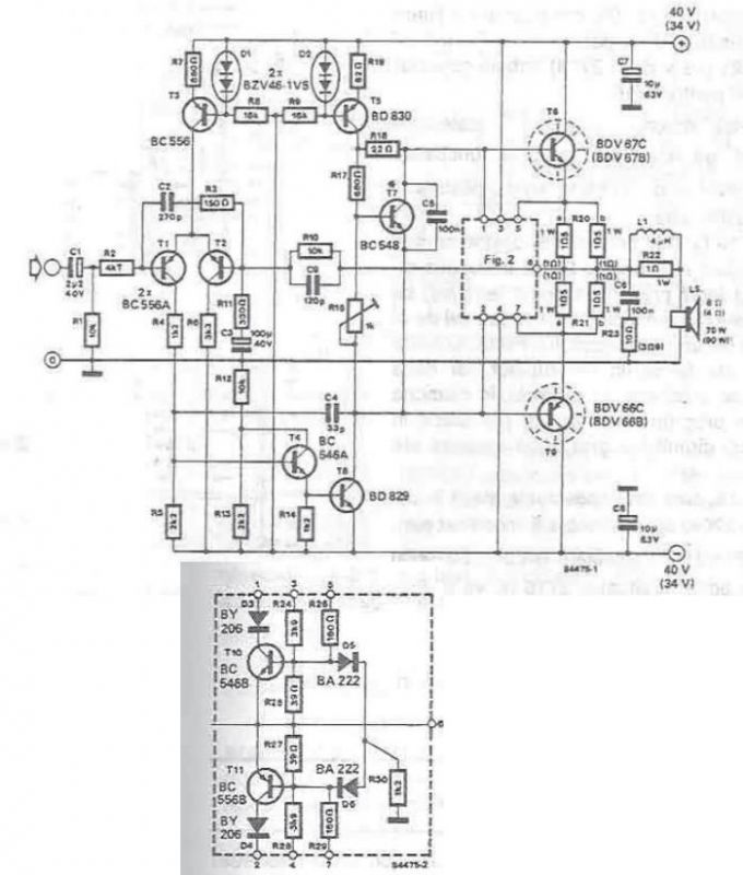
Power amplifier using transistors
A high-power audio amplifier can be designed using power transistors and other common electronic components, capable of delivering a maximum output power of 90W. When using the specified component values, it can drive speakers with a 4-ohm impedance, resulting in...
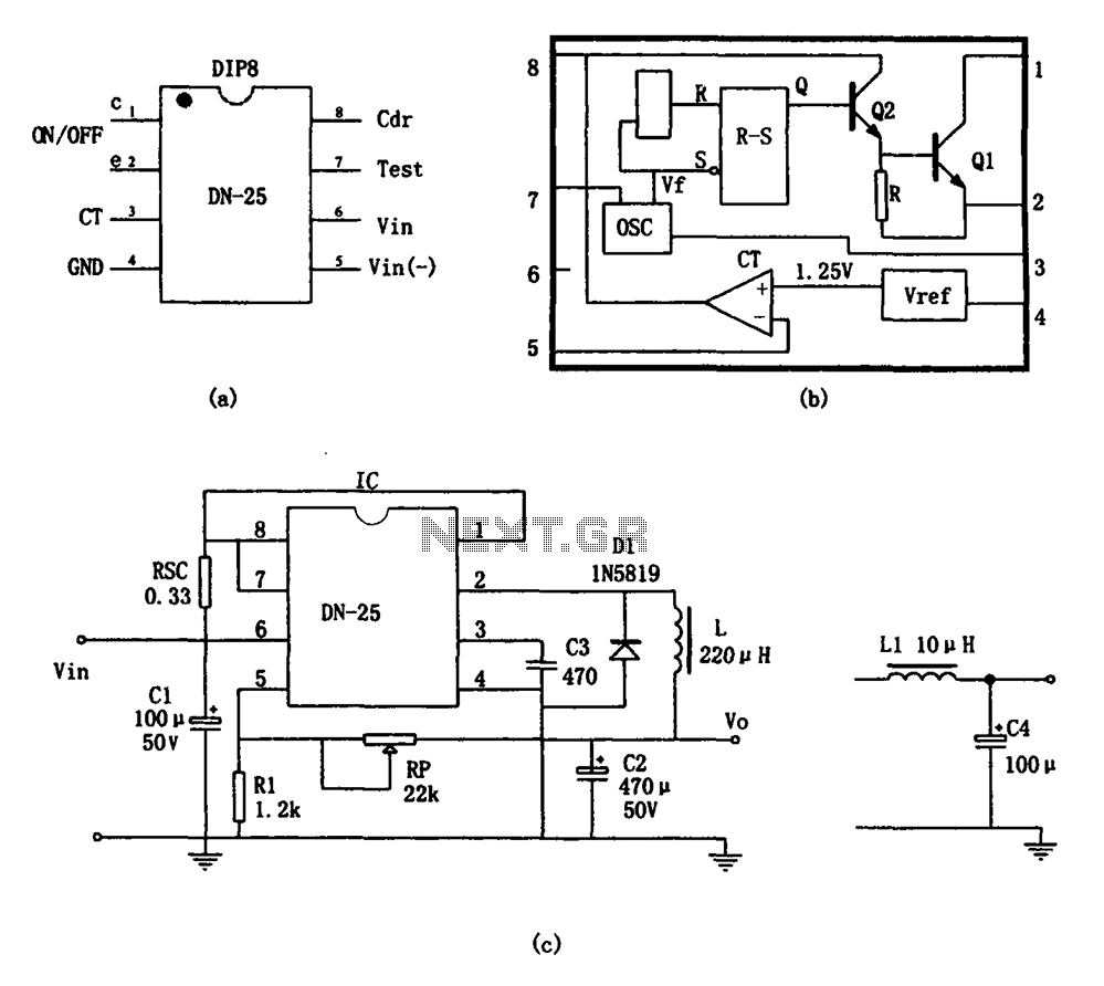
Switching power supply monolithic switching regulator DN-25 configuration
As shown in the figure, the DN-25 IC is a switching power supply. The DN-25 is a monolithic switching power supply device suitable for medium output current applications and a wide voltage range. Its main performance indicators include an input...
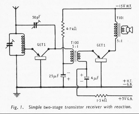
early GEC transistor radio
The world's first practical crystal amplifying device was introduced in 1948, marking the beginning of commercially available transistor radios in Britain. At that time, an average radio enthusiast or constructor would have been adjusting to new miniature glass valves, exploring...
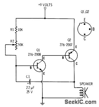
transistors How does this circuit diagram work
R2 controls the charging speed of capacitor C1. At a specific charge level, C1 triggers transistors Q1 and Q2, which release a 9-volt pulse. This pulse generates a clicking sound. The discharge process of the capacitor involves it charging gradually...
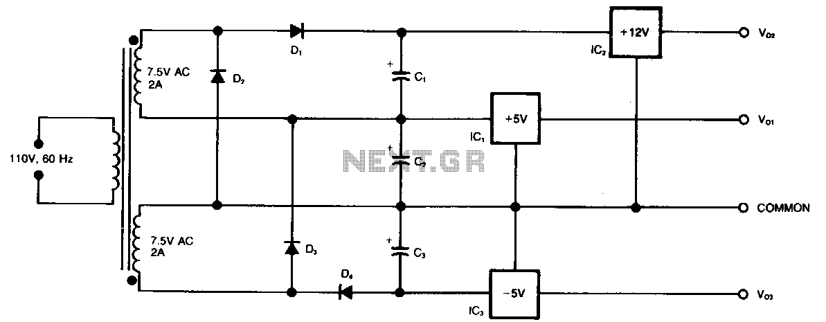
Three-rail-power-supply
This circuit generates three supply voltages using a minimal number of components. Diodes D2 and D3 perform full-wave rectification, alternately charging capacitor C2 during both halves of the AC cycle. Meanwhile, diode D1 in conjunction with capacitor C1, and diode...