


High voltage stabilizing circuit diagram composed of optocouplers
#optocoupler
#high voltage
#stabilizing circuit
#transistor
#voltage regulation
#breakdown voltage
#bias
#9013 transistor
#output voltage
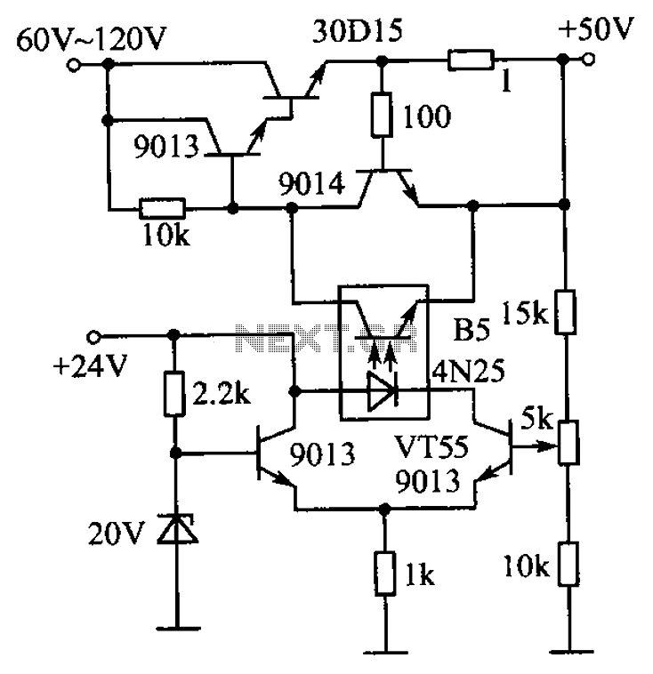
Description: The circuit is illustrated. A standard driving transistor requires a higher breakdown voltage transistor (such as the FIG driving tube 9013). As the output voltage rises, the bias on VT55 increases, leading to an increase in the forward current of the light-emitting diode. This causes the voltage across the photodiode to decrease, which in turn biases the regulator to reduce junction resistance, resulting in a decrease in output voltage. Conversely, when the output voltage increases, the system works to maintain a stable output voltage.
The described circuit operates with a focus on maintaining stable output voltage levels through feedback mechanisms involving various components. The use of a driving transistor with a higher breakdown voltage, such as the 9013, is critical for ensuring reliable operation under higher voltage conditions. The transistor VT55 plays a pivotal role in the circuit's performance as it regulates the biasing conditions.
When the output voltage increases, the forward current through the light-emitting diode (LED) also rises. This increase in current is significant as it affects the voltage across the photodiode, which is a key component in the feedback loop of the circuit. The reduction in voltage across the photodiode leads to a decrease in the biasing current for the regulator. This action effectively reduces the junction resistance within the regulator, which in turn causes the output voltage to decrease.
The feedback mechanism is essential for ensuring that the output voltage remains stable despite fluctuations in load conditions or input voltage variations. If the output voltage begins to rise excessively, the circuit automatically compensates by adjusting the biasing conditions, thereby preventing overvoltage situations. This self-regulating behavior is crucial for applications requiring consistent voltage levels, such as in power supply circuits or LED drivers.
Overall, the circuit exemplifies a robust design that utilizes feedback from the LED and photodiode to maintain output stability, ensuring reliable operation across varying conditions. The careful selection of components, such as the high breakdown voltage transistor and the configuration of the feedback loop, contributes to the overall effectiveness of the circuit in achieving its intended performance objectives. Circuit is shown. Normal driving transistor would need a higher breakdown voltage transistor (FIG driving tube 9013). When the output voltage increases, VT55 bias increases, B5 light emitting diode forward current increases, the voltage between the photodiode decreases, the regulator be biased to reduce junction resistance increases and the output voltage decreases ; on the contrary, the output voltage increases, thereby maintaining a stable output voltage.
The described circuit operates with a focus on maintaining stable output voltage levels through feedback mechanisms involving various components. The use of a driving transistor with a higher breakdown voltage, such as the 9013, is critical for ensuring reliable operation under higher voltage conditions. The transistor VT55 plays a pivotal role in the circuit's performance as it regulates the biasing conditions.
When the output voltage increases, the forward current through the light-emitting diode (LED) also rises. This increase in current is significant as it affects the voltage across the photodiode, which is a key component in the feedback loop of the circuit. The reduction in voltage across the photodiode leads to a decrease in the biasing current for the regulator. This action effectively reduces the junction resistance within the regulator, which in turn causes the output voltage to decrease.
The feedback mechanism is essential for ensuring that the output voltage remains stable despite fluctuations in load conditions or input voltage variations. If the output voltage begins to rise excessively, the circuit automatically compensates by adjusting the biasing conditions, thereby preventing overvoltage situations. This self-regulating behavior is crucial for applications requiring consistent voltage levels, such as in power supply circuits or LED drivers.
Overall, the circuit exemplifies a robust design that utilizes feedback from the LED and photodiode to maintain output stability, ensuring reliable operation across varying conditions. The careful selection of components, such as the high breakdown voltage transistor and the configuration of the feedback loop, contributes to the overall effectiveness of the circuit in achieving its intended performance objectives. Circuit is shown. Normal driving transistor would need a higher breakdown voltage transistor (FIG driving tube 9013). When the output voltage increases, VT55 bias increases, B5 light emitting diode forward current increases, the voltage between the photodiode decreases, the regulator be biased to reduce junction resistance increases and the output voltage decreases ; on the contrary, the output voltage increases, thereby maintaining a stable output voltage.
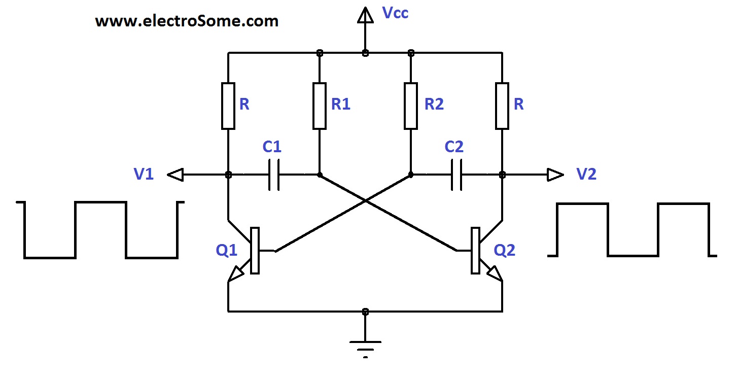
astable multivibrator transistors
An astable multivibrator, also known as a free-running multivibrator, is a circuit that does not have stable states. Its output oscillates continuously between two unstable states without requiring external triggering. The duration of each state is determined by the resistor-capacitor...
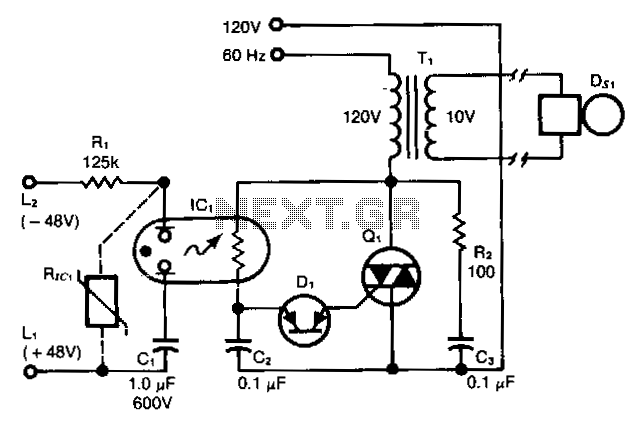
Optically-int-erfaced-ring-detector
This ring detector, utilizing a neon-LDR (light-dependent resistor) optocoupler, simplifies interfacing with telephone lines.
The ring detector circuit is designed to detect the ringing signal from telephone lines, which typically operates at a frequency of 20 Hz to 25 Hz with...
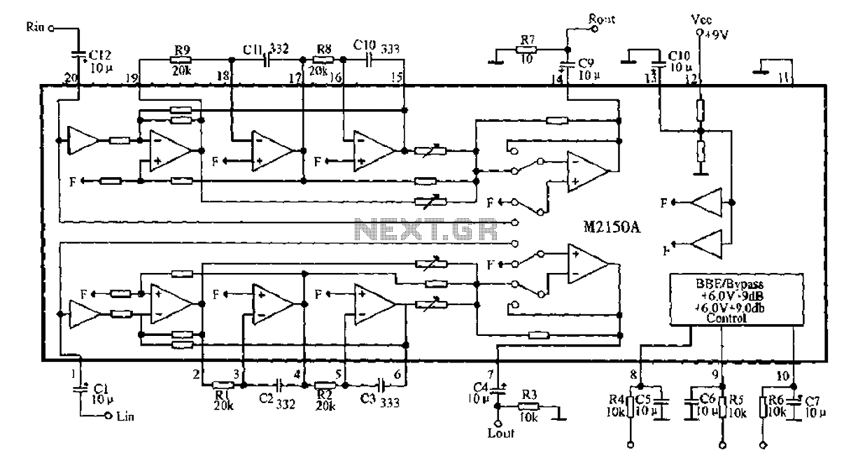
BBE monolithic integrated circuit M2150A
4V flat monitor high voltage power supply circuit diagram. A wide range of 7 to 40V to 5V DC-DC step-down circuit diagram. Light control switch circuit diagram for safety. Circuit 555 constitutes a control circuit diagram for photoelectric applications.
The 4V...
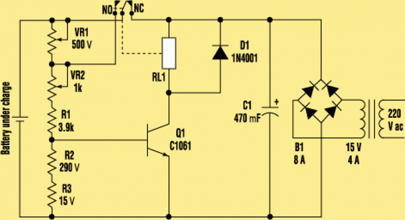
a single transistor smart battery charger
The electronic design features a smart battery charger schematic that utilizes only a single transistor. This design is notable as similar circuits typically employ simple integrated circuits. When the battery's charge level falls below a specific threshold voltage, the circuit...

High Voltage Power Supply for Valve Preamplifiers
The amplifier feeding the final amplification stage operates with unstabilized voltage. The output stage, utilizing push-pull operation, exhibits significant rejection of the supply voltage. However, the earlier stages do not provide the same level of rejection, resulting in unwanted noise....
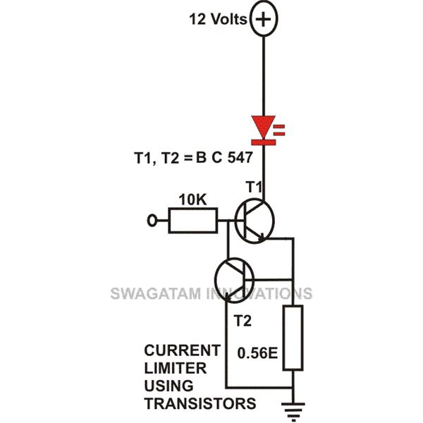
basic transistor circuits for beginners explored
This article compiles small transistor circuits and configurations suitable for beginners, including current amplifiers, limiters, oscillators, and latches. A simple current amplifier circuit can be constructed using just a couple of NPN transistors. Additionally, two transistors and resistors can be...
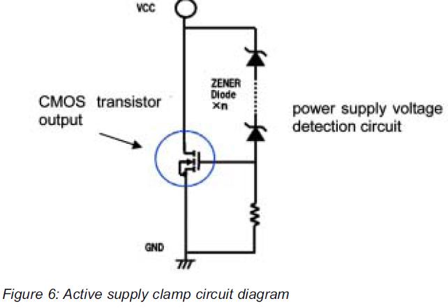
High Reliability for 1200V High Voltage Integrated Circuit for Half Bridge Applications
This article presents a high reliability 1200V High Voltage Integrated Circuit (1200V HVIC) for half bridge driver applications, aimed at reducing the IC's supply current by approximately 50%.
The 1200V High Voltage Integrated Circuit (HVIC) is designed specifically for half-bridge driver...
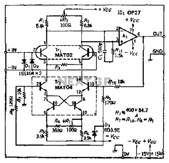
Double transistor low noise of the preamplifier measured by high
The Bong ordinary differential amplifier circuit differs from a standard differential circuit by incorporating a voltage-current conversion circuit, which consists of resistors R and Rl. The operational amplifier (OP amp) includes a voltage divider that subsequently converts the voltage into...
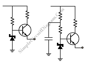
Transistor Buffer for Zener Diode Voltage Regulator
Buffering for the zener diode is achieved through the impedance matching and current amplifying features of the emitter follower, which draws less current from the zener.
Buffering in electronic circuits is essential for ensuring that the performance of one component does...