
clap sensor construction
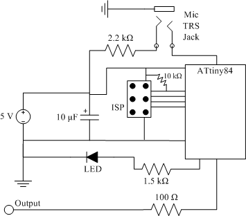
The clap sensor circuit effectively utilizes a combination of components to achieve its intended functionality. The choice of the ATtiny84 microcontroller allows for efficient processing of input signals from the microphone, which captures sound and converts it into an electrical signal. The use of a TRS jack simplifies the connection of the microphone, ensuring reliable signal transmission while minimizing the footprint on the circuit board.
The 2.2 kΩ resistor connected to the ring conductor is critical for biasing the microphone, preventing the output signal from floating and ensuring a stable reading. The 10 µF capacitor serves as a power filter, smoothing out any fluctuations in the power supply that could affect the performance of the microcontroller and other components.
The incorporation of an LED provides immediate visual feedback, enhancing the user interface. The choice of a high-value current-limiting resistor is indicative of the design's consideration for power efficiency, especially when using low-current LEDs.
The ISP connector's design facilitates easy programming and debugging of the microcontroller. The AVRISP mkII programmer allows for straightforward code uploads, essential for developing and testing the circuit functionality. The design also includes provisions for a pull-up resistor on the RESET pin, which is crucial for ensuring the microcontroller operates correctly without unintended resets during normal operation.
The printed circuit board (PCB) design reflects careful planning, with the layout optimized for both component placement and signal integrity. The two-layer configuration allows for a compact design while maintaining separation between power and signal traces, reducing the likelihood of interference. The design choices made in terms of hole sizes and trace widths demonstrate a thorough understanding of standard PCB manufacturing practices, ensuring compatibility with commonly available components.
Overall, this clap sensor circuit exemplifies a well-thought-out design that balances functionality, size, and ease of use, making it a suitable project for both educational purposes and practical applications.The clap sensor is a simple circuit that incorporates a PC microphone, a microcontroller, and an output. The following diagram shows the logical circuit design: I chose the ATtiny84 microcontroller for this project because I`m familiar with the AVRarchitecture and Ihave access to the tools to use it.
I bought the ATtiny84 in its SOIC-14 packaging. If Ihad it to do again then I`d choose the ATtiny85, which comes in a SOIC-8 package; it contains all the features Ineeded but takes up less space. It`s not a real problem though. The microphone connects to the circuit through a tip-ring-sleeve (TRS) jack. I chose the SJ1-3533N jack from CUI Inc. because it looks nice and has a small footprint on the circuit board. It breaks out the tip, ring and sleeve conductors on three pins on the bottom. The sleeve conductor is connected to ground, and the ring is connected to V+ through a 2. 2 k © resistor (without this resistor the microphone`s output signal is constant). The tip conductor carries the microphone`s output signal. The circuit`s 10 F capacitor filters the power input. The LED is for visual output. The LED`s current-limiting resistor value, in the diagram labeled 1. 5 k ©, depends on the LED. I used a low-current LED, so the resistance is quite high. The resistor value for other LEDs can be calculated with this tool, with the source voltage value set to the input voltage (5 Vin my circuit) and the diode voltage and current taken from the LED`s datasheet.
The six-pin connector next to the ATtiny84 in the circuit diagram is for the in-system programmer(ISP), which is how code is loaded onto theATtiny84. I used Atmel`s AVRISPmkII to load code. The following diagram shows theISPpinout on the header: The ISP interface corresponds to a serial peripheral interface (SPI)connection; the only difference is that themicrocontroller can be put into programming mode while the RESET pin is held low.
This is all handled automatically by the AVRISP driver. The Vcc and GNDpins have to be connected to external power. Also, the RESET pin must be connected to Vcc through a 10 k © pullup resistor as shown in the circuit diagram above, to keepRESEThigh when the processor is running. The header`s pins are connected to pins on the microcontroller. The microcontroller pins are labeled with their SPI(and RESET) designations in the microcontroller`s data sheet.
For theATtiny84, the datasheet [PDF] gives the pin designations on page 2: I designed the circuit board using a program called ExpressPCB. It`s not the most complete design program and it uses a proprietary file format that doesn`t work with other software, but it`s very easy to use and is well-documented.
I designed the two-layer circuit board below; the red traces are the top copper layer, the green traces are the bottom copper layer, and the yellow is for silkscreened information(Idon`t print the silkscreen layer, but it`s shown below for informational purposes). The large holes fit standard 0. 1 ³ headers; they have a 1. 91 mm outer diameter and 1. 02 mm inner diameter. The small holes fit component leads; they have a 1. 42 mm outer diameter and a 0. 74 mm inner diameter. The small holes on the CPU are just through-holes that connect the bottom layer copper to the top. The three resistor spots in the bottom-left corner of the board are sized for 1/4 W resistors. The three 0. 1 ³ pins in the upper-left corner are, from top to bottom, for V+, GND, and the output. The ISPheader is oriented with pin 1 at the top-left. This design doesn`t include the ISP port`s pullup resistor. I couldn`t figure out how to fit it onto the board. If Iwas going to make another version of the board I would put a surface-mount resistor between the Vcc and RESET pins to the right of the ISPport.
I ended up using a 1/4 W resistor soldered above the board, between the Vcc trace and the through-hole connected to the RESET pin. I used instructions written by Chris 🔗 External reference
Related Circuits

Mindsensors produces an excellent RCX sensor multiplexer for the NXT, known as the RXMux, which enables the connection of up to four RCX-style analog sensors to the NXT. The RXMux supports various sensors. Due to the frequent use of...
A single hand clap will be picked up by the electric mic which is coupled through C1 into the op amp IC1. The output of IC1 triggers the 555 IC timer IC2 which is configured as a monostable multivibrator....
A project involving a moisture sensor alarm circuit designed to detect moisture levels in plant soil, wood, and irrigation areas. The moisture sensor alarm circuit typically consists of a moisture sensor, a microcontroller or comparator circuit, an alarm system, and...

The LM35 series are precision integrated-circuit temperature sensors, whose output voltage is linearly proportional to the Celsius (Centigrade) temperature. The LM35 has an advantage over linear temperature sensors calibrated in Kelvin, as the user is not required to subtract...
Parts List The circuit was specifically designed for shop window animation as it utilizes a capacitive sensor that is activated by a touch control system. The circuit is intended for enhancing visual displays in retail environments by creating dynamic animations...

The 1B32 application circuit features multiple pressure sensors as illustrated in the figure. Excitation power is supplied through the AD542, which is followed by a TIP32 transistor that drives multiple bridge sensors. The AD542 operates as a Bi-FET in...
Warning: include(partials/cookie-banner.php): Failed to open stream: Permission denied in /var/www/html/nextgr/view-circuit.php on line 713
Warning: include(): Failed opening 'partials/cookie-banner.php' for inclusion (include_path='.:/usr/share/php') in /var/www/html/nextgr/view-circuit.php on line 713