Class B Amplifier
1. Definition and Working Principle
1.1 Definition and Working Principle
A Class B amplifier, which is a pivotal element within the realm of analog electronics, operates as a voltage amplification device where the output signal is proportional to the input signal. This class of amplifier is characterized by its conduction mechanism in which each active device (transistor) conducts for exactly half of the input signal cycle. As a result, Class B amplifiers are particularly efficient and produce less heat than their Class A counterparts, although they do introduce some distortion due to their turn-on and turn-off properties.
The operation of a Class B amplifier typically involves two complementary transistors—one NPN and one PNP—arranged in a push-pull configuration. This arrangement allows for the effective amplification of both halves of the waveform, effectively doubling the efficiency while maintaining a level of fidelity that is acceptable for many applications.
The Working Mechanism
To explore the working principle of a Class B amplifier, it’s essential to look at its signal processing capabilities. Each transistor is biased at a point just below the cutoff point; it does not conduct during the entire cycle. As the input AC signal is applied, it swings above and below ground. The NPN transistor conducts during the positive half-cycle of the input signal, while the PNP transistor takes over during the negative half-cycle. This push-pull arrangement ensures that the output is a faithful reproduction of the input signal but in a significantly amplified form.
In terms of mathematical representation, the relationship governing the output is as follows:
Here, \( \beta \) represents the current gain of the transistors, \( V_{in} \) is the amplitude of the input signal, and \( V_{be} \) is the base-emitter junction voltage, which is typically around 0.7V for silicon transistors. This basic equation illustrates how the input voltage is scaled, leading to the output voltage being magnified according to the characteristics of the transistors used.
Efficiency and Applications
Class B amplifiers achieve a theoretical maximum efficiency of around 78.5%. This is derived from the ratio of the output power to the total power consumed under ideal conditions. This efficiency, coupled with the ability to handle high power outputs, makes Class B amplifiers suitable for a variety of applications, including:
- Audio Amplification: Widely used in audio equipment where high efficiency and acceptable sound quality are required.
- Radio Frequency Transmission: Employed in RF transmitters where output power efficiency is crucial.
- Switching Power Supplies: Utilized in power conversion circuits that require efficient designs.
The trade-off, however, lies in the inherent distortion—a phenomenon known as crossover distortion—caused by the non-conduction of the transistors during the zero crossover point. This necessitates careful design considerations and sometimes the use of feedback techniques to mitigate such effects, thereby enhancing the overall linearity and performance of the amplifier.
In conclusion, the Class B amplifier offers an intriguing mixture of efficiency, simplicity, and practical application potential. Understanding its operation not only enhances the comprehension of amplifier design but also serves as a foundational element for further exploration into more complex amplification systems.
1.2 Advantages and Disadvantages
The Class B amplifier, a staple in audio and RF applications, exhibits unique characteristics that make it suitable for various contexts. However, its performance comes with both strengths and weaknesses. A thorough understanding of these advantages and disadvantages can enhance the design and implementation of audio systems and other applications dependent on amplification.Advantages of Class B Amplifiers
One of the primary advantages of Class B amplifiers is their efficiency. Unlike Class A amplifiers, which conduct over the entire input cycle, Class B amplifiers only conduct for half of the input signal cycle. This property leads to a higher efficiency rate, generally around 60-70%, compared to the meager 25-30% often seen in Class A designs. Such efficiency makes Class B amplifiers highly favorable for battery-powered devices and environments where thermal management is critical. Another crucial advantage is the reduced crossover distortion that comes from proper biasing. In a perfectly designed Class B amplifier, the transistor conducts only during one half of the waveform. This can be advantageous in audio applications, where minimizing distortion is paramount. Additionally, using complementary push-pull pairs of transistors can further reduce this distortion, providing a more accurate representation of the input signal. Moreover, Class B amplifiers can handle a significant level of input signal without distortion, making them suitable for high-power applications. This capability allows for the amplification of various audio signals and radio frequencies that require robust performance without sacrificing fidelity.Disadvantages of Class B Amplifiers
Despite their advantages, Class B amplifiers also have notable drawbacks. The operating principle of each transistor conducting for only half of the input waveform implies the potential for crossover distortion, particularly at low signal levels. While techniques exist to mitigate this (such as using negative feedback), addressing this issue is crucial in applications requiring high linearity. Class B amplifiers also demand careful thermal management. Although they generate less heat than Class A amplifiers, they still produce significant heat during operation. If not appropriately managed, this heat can lead to transistor degradation or overall amplifier failure. Moreover, the design complexity increases due to the need for complementary transistors and additional circuitry to minimize distortion. This additional complexity can lead to higher costs and longer development times in the design phase, particularly in tightly controlled environments or in consumer applications where price is a significant factor.Practical Relevance and Applications
Class B amplifiers find extensive use in audio amplification systems such as home theater systems, musical instrument amplifiers, and public announcement systems, where their high efficiency and power capabilities provide tangible benefits. The balance of efficiency and performance makes them popular in RF applications as well, specifically in transmitters where power management is critical. In summary, understanding the advantages and disadvantages of Class B amplifiers enables engineers and designers to make informed decisions based on application-specific requirements. As technology advances, ongoing research continues to address the limitations of Class B amplifiers, leading to innovations that propel their functionality even further.1.3 Applications of Class B Amplifiers
Class B amplifiers, characterized by their operation in the linear region for half of the input signal waveform, have found widespread applications across various fields due to their efficiency and simplicity. Their ability to amplify signals without substantial distortion while maintaining a relatively low power consumption profile makes them ideal for a range of practical uses. One of the most prominent applications of Class B amplifiers is in audio amplification systems. In these systems, two complementary transistors are utilized to ensure that each handles only half of the input signal cycle. This configuration not only optimizes power usage but also minimizes the thermal output of the transistors, as they are not continuously conducting. This makes Class B amplifiers especially suitable for driving loudspeakers in home audio systems, public address systems, and musical instrument amplifiers. Beyond audio systems, Class B amplifiers are also extensively used in RF (radio frequency) applications. The high efficiency of Class B amplifiers allows for the transmission of RF signals over long distances, making them vital components in communication systems, such as those utilized in broadcasting and mobile communications. The reduction of heat generation is particularly valuable in these applications, as transistors can operate reliably even under demanding conditions without the need for extensive cooling solutions. The field of industrial control also leverages Class B amplifiers. Here, they are instrumental in driving actuators and motors, where high efficiency translates directly into lower operational costs. In robotics, Class B amplifiers can manage the power supply to servos and other drive components, highlighting their versatility in real-time control systems that require precise signal handling without significant power loss. In the realm of instrumentation, Class B amplifiers are frequently employed in signal processing applications. Their capability to efficiently amplify small signals from sensors and transducers enables accurate readings in diverse applications, such as medical instrumentation, environmental monitoring, and industrial automation. The linear response of Class B amplifiers in the small signal range ensures that they can provide high fidelity output necessary for these critical measurements. Despite their advantages, Class B amplifiers also face challenges, particularly concerning crossover distortion, as the output signal transitions between the two transistors. This phenomenon occurs at the point where both transistors are off, leading to a slight delay before the active transistor begins to conduct. Techniques such as negative feedback, biasing adjustments, and the implementation of Class AB designs—where each transistor operates slightly more than half the cycle—are often employed to mitigate these effects, further expanding the utility of Class B configurations in precision applications. In summary, Class B amplifiers are foundational components in a variety of domains ranging from audio engineering to telecommunications and industrial automation. Their efficiency and effectiveness in amplifying signals without excessive distortion make them indispensable in today’s technology-driven environments. As advancements in materials and circuit design continue, the applications of Class B amplifiers are expected to grow, further transcending traditional boundaries and fostering innovations in electronic design.2. Basic Class B Amplifier Circuit
2.1 Basic Class B Amplifier Circuit
The Class B amplifier is a crucial building block in modern electronics, particularly in audio amplification and RF applications, due to its efficiency and ability to handle high power levels. The basic configuration of a Class B amplifier employs two active devices, typically bipolar junction transistors (BJTs) or field-effect transistors (FETs), which work in a push-pull arrangement. This design enables the amplification of both halves of the input signal while mitigating distortion. In this subsection, we will explore the fundamental circuit design and operation principles of a Class B amplifier.
Operating Principle of Class B Amplifiers
Class B amplifiers operate such that each transistor conducts for exactly half of the input signal cycle. As one transistor amplifies the positive half-cycle, the other remains off and vice versa for the negative half-cycle. This complementary operation not only improves the linearity of the output but also enhances the overall efficiency. The mathematical representation of this can be illustrated as follows:
Here, \( P_{out} \) represents the output power, \( V_{cc} \) is the supply voltage, and \( R_L \) is the load resistance. To maximize the output efficiency, the theoretical efficiency of a Class B amplifier can be derived as:
This indicates that Class B amplifiers can provide an efficiency of around 50%, significantly higher than that of Class A amplifiers, which operate at around 25% efficiency. However, they do introduce some distortion known as crossover distortion due to the non-conduction point where the transistors transition. This operational characteristic is critical when considering Class B amplifiers for applications requiring high fidelity.
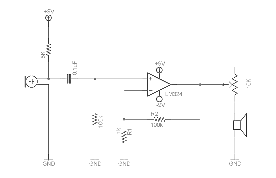
Basic Circuit Diagram
The typical basic Class B amplifier circuit consists of two transistors connected to a common load resistor. The transistors are configured to work in a push-pull arrangement and are often biased slightly above cutoff to minimize crossover distortion. Below is a description of how this setup is organized:
The circuit comprises:
- Two Transistors: One NPN and one PNP transistor are used to handle the positive and negative halves of the input signal, ensuring a continuous signal flow.
- Biasing Resistors: To set the quiescent operating point slightly above cutoff, resistors may be connected to the base terminals of the transistors.
- Load Resistor: This is connected at the output, typically represented as \( R_L \), which is responsible for converting the amplified output into usable power.
The following diagram illustrates a basic Class B amplifier circuit:
Understanding this basic setup allows engineers to modify the amplifier circuit for various applications, aiming either for higher output power or lower distortion levels depending on the requirement.
Applications and Considerations
Class B amplifiers are frequently utilized in large audio systems where efficiency is paramount. They are also significant in RF applications, where they can drive transmitters with minimal power loss. Despite their advantages, careful consideration must be given to biasing and component selection to minimize distortion and ensure stability across varying temperatures and loads.
As the demand for efficient amplification grows in modern electronics, Class B amplifiers will continue to play a vital role, paving the way for advancements in audio technology and beyond.
2.2 Push-Pull Configuration
In the domain of Class B amplification, the push-pull configuration stands as a pivotal concept, effectively maximizing power efficiency while minimizing distortion. This configuration typically employs two complementary transistors—one NPN and one PNP—operating in tandem to amplify both halves of an input signal.Principle of Operation
The push-pull configuration achieves its functionality by alternating the duty cycle between the two transistors. During the positive half-cycle of the input signal, the NPN transistor conducts, allowing current to flow through the load, while the PNP transistor remains off. Conversely, during the negative half-cycle, the roles reverse, with the PNP transistor taking over the conduction. This arrangement ensures that both halves of the waveform are amplified, which is essential for applications requiring high fidelity, such as audio amplification.Mathematical Representation
To delineate the current and voltage behaviors in a simplified push-pull amplifier circuit, we can derive relevant equations that express these characteristics. For a resistive load \( R_L \), the output voltage \( V_{out} \) can be expressed as: $$ V_{out} = I_{C1} \cdot R_L \quad \text{(for NPN on)} $$ and $$ V_{out} = I_{C2} \cdot R_L \quad \text{(for PNP on)} $$ By recognizing that the collector currents \( I_{C1} \) and \( I_{C2} \) are the same magnitude yet opposite in direction, we can combine these representations over one complete cycle. Thus, we can say: $$ I_{C1} = I_{C2} = I_{C} $$ The average output voltage over a full cycle can be given by: $$ V_{avg} = \frac{1}{T} \int_0^T V_{out}(t) \, dt $$ With \( T \) being the time period of the input signal. Applying this to our push-pull configuration, we notice that efficient power handling occurs, leading to minimal crossover distortion primarily attributed to the non-conductive periods.Advantages
The push-pull configuration in Class B amplifiers offers several notable advantages:- Higher Efficiency: Typically around 78.5%, which is significantly better than Class A amplifiers.
- Reduction in Distortion: The use of two complementary devices helps minimize the effects of crossover distortion, which is a common issue in single-ended amplifiers.
- Thermal Stability: Due to the complementary nature of the transistors, variations in temperature will have a more balanced impact, improving reliability.
Practical Applications
The implications of the push-pull configuration are vast and pervasive in real-world scenarios. For instance, audio power amplifiers in sound systems utilize this configuration to drive loudspeakers efficiently, while various electronic devices, such as radio-frequency transmitters and operational amplifiers, exploit the benefits of this topology. Its effectiveness in ensuring fidelity in audio applications makes it a cornerstone in both consumer and professional audio engineering.Conclusion
In summary, the push-pull configuration is integral to the performance of Class B amplifiers, enhancing efficiency and linearity while mitigating common distortion problems. Understanding its operational mechanics paves the way for sophisticated applications and innovations in electronic design, allowing engineers and physicists to harness its potential in various fields.2.3 Biasing Techniques
In the realm of Class B amplifiers, effective biasing techniques are crucial for optimal performance. Biasing ensures that the transistors operate in the active region, allowing for linear amplification of the input signal. This section delves into the various techniques employed to achieve proper biasing in Class B amplifiers, their advantages, disadvantages, and practical applications.
Understanding Biasing
Biasing, in an electronic circuit, refers to the process of setting a predefined voltage or current to establish the operating point of an electronic device, typically a transistor. For a Class B amplifier, it is essential to set the bias point such that the transistor only conducts during half of the input signal cycle. This contrasts with Class A amplifiers where biasing is set to allow full conduction at all times, thus resulting in higher power dissipation.
Key Biasing Techniques
Several techniques can be employed for biasing Class B amplifiers, each with distinct characteristics:
- Fixed Biasing: In this method, a fixed resistance is connected to the base of the transistor to establish a constant base current. While simple, it is sensitive to temperature variations which can lead to drift in the operating point.
- Emitter Biasing: Adding a resistor in the emitter path stabilizes the operating point against temperature changes. The addition of this resistor introduces negative feedback, which improves linearity, albeit at the cost of reduced gain.
- Voltage Divider Biasing: This technique employs two resistors in a voltage divider network connected to the base. It provides stable biasing independent of beta variations, making it a popular choice for ensuring consistent performance.
- Self-Biasing: Also known as temperature-compensated biasing, this technique uses feedback from the output to maintain the desired biasing conditions. This is particularly effective at balancing variations in temperature and device characteristics.
Comparative Analysis
When selecting a biasing method, it is essential to consider its implications on performance:
- Fixed Biasing offers simplicity but lacks thermal stability.
- Emitter Biasing enhances stability but incurs a slight gain reduction.
- Voltage Divider Biasing ensures more consistent performance, making it ideal for most applications.
- Self-Biasing allows for dynamic adjustments but may increase circuit complexity.
Mathematical Consideration
To illustrate the impact of these techniques, consider the calculation of the quiescent current and voltage:
For a basic Class B amplifier biased through a voltage divider, the base voltage \( V_B \) can be expressed as:
Where:
- R1 and R2 are the resistances of the voltage divider.
- VCC is the supply voltage.
This voltage will determine the emitter current, calculated via:
Where:
- VBE is the base-emitter voltage (typically 0.7V for silicon transistors).
- RE is the emitter resistor.
The resulting collector current \( I_C \) can then be derived directly from \( I_E \) in Class B operation, as \( I_C \) closely approximates \( I_E \) in terms of the magnitude.
Practical Applications and Considerations
Choosing the right biasing technique is pivotal for applications ranging from audio amplification to RF transmission. A well-biased Class B amplifier can efficiently drive speakers, resulting in high linearity with minimal distortion. Further, advancements in integrated circuit technology have enabled biasing techniques to be implemented within the semiconductor design, mitigating traditional challenges.
In conclusion, understanding and implementing appropriate biasing techniques is imperative for optimizing Class B amplifier performance, with each method presenting unique trade-offs that can significantly impact circuit functionality.
3. Input and Output Characteristics
3.1 Input and Output Characteristics
The Class B amplifier is distinctive for its efficiency and linearity, traits that stem from its foundational operation principles. Understanding the input and output characteristics of a Class B amplifier is crucial for engineers and researchers alike, as these characteristics directly influence performance metrics such as gain, distortion, and bandwidth.
At the heart of a Class B amplifier's operation lies its configuration utilizing two complementary transistors—NPN and PNP. Each transistor conducts for half of the input signal cycle, which assists in minimizing power dissipation compared to Class A amplifiers. To delve into the input and output characteristics, we examine both the voltage and current behavior.
Input Characteristics
The input characteristic curve provides insight into how the amplifier responds to varying input signals. When the input voltage is applied, the output characteristics of each transistor are segmented into two operating regions, effectively limiting the conduction to half the input signal cycle.
Typically, the input characteristics can be plotted as a graph with the input current (IB) on the x-axis and the input voltage (VBE) on the y-axis. The curve is usually a straight line that indicates the base-emitter voltage required for a specific base current:
where:
- VBE = base-emitter voltage
- VT = thermal voltage (approximately 26 mV at room temperature)
- IS = saturation current
- IC = collector current
Because the Class B amplifier conducts only during half of the input cycle, it also exhibits high input impedance, making it suitable for interfacing with high-impedance sources.
Output Characteristics
The output characteristic curves of a Class B amplifier showcase how output voltage and current behave with respect to varying input. To visualize this behavior, we typically plot the collector current (IC) against the collector-emitter voltage (VCE).
In the output characteristics, you will see different regions, including the active region, which for the Class B amplifier consists of the quadrant where both transistors operate in their linear region:
This equation implies the development of a voltage drop across the load resistor (RC), dependent on the load current. A distinguishing feature of the Class B amplifier is the introduction of significant crossover distortion during the transition between the two conduction halves. This arises because neither transistor will conduct perfectly at the zero-crossing point of the input signal, leading to nonlinearities.
Key Points and Practical Applications
- Efficient power usage: Class B amplifiers can achieve up to 78.5% theoretical efficiency, making them preferred in battery-operated devices.
- Low distortion: Proper biasing and feedback mechanisms are essential for minimizing crossover distortion, crucial in high-fidelity audio applications.
- Temperature stability: Designing Class B amplifiers with thermal management ensures consistent performance over a broad range of operating conditions.
In summary, analyzing the input and output characteristics of Class B amplifiers provides essential insights into their operation. This analysis is vital for applications in audio systems, communication devices, and signal processing circuits, where linearity and efficiency are paramount.
3.2 Efficiency and Linearity
The Class B amplifier configuration is notorious for achieving a desirable balance between efficiency and linearity, making it a popular choice for various applications including audio amplification and radio frequency processing. Understanding the complexities of these two aspects is crucial for optimizing performance in practical applications. To begin with, let us consider efficiency, a vital parameter for amplifiers, defined as the ratio of output power to input power. For a Class B amplifier, the maximum theoretical efficiency can be expressed as: $$ \eta_{max} = \frac{P_{out}}{P_{in}} \times 100\% $$ In a sine wave approximation, this efficiency can reach up to approximately 78.5%. This impressive figure derives from the fact that each transistor in the output stage conducts for half of the input signal cycle, minimizing the total power dissipation. Such behavior allows the Class B configuration to utilize power effectively, particularly advantageous in battery-powered devices and applications with strict thermal limitations. However, this pursuit of efficiency inevitably raises concerns regarding linearity. Linearity in amplifiers refers to the extent to which the output signal faithfully reproduces the input signal without distortion. For Class B amplifiers, during the critical transition between positive and negative cycles, linear performance is challenged. As the amp shifts from one transistor to the other, a phenomenon known as "crossover distortion" occurs. This type of distortion arises because there is a brief period where neither transistor is conducting, resulting in a distortion of the output waveform. To quantify this distortion, you can examine the output characteristics of a Class B amplifier, which can be visualized in a graph where the x-axis represents the input voltage and the y-axis shows the output voltage. The nonlinearities around the axis crossing will depict the distortion. In practical terms, engineers may employ various techniques to mitigate crossover distortion, like employing a biasing circuit to allow both transistors to conduct slightly during cutoff, thus ensuring a smoother transition at the point where they cross. This adjustment can slightly reduce amplifier efficiency but significantly enhance linearity. To summarize, the trade-off between efficiency and linearity in Class B amplifiers highlights core design challenges. While these amplifiers can achieve remarkable efficiency, careful consideration must always be given to linearity to prevent unwanted distortion, especially critical in high-fidelity audio applications. Understanding these intricate relationships prepares engineers to tailor solutions across diverse applications—from home audio systems to complex RF transmitters—where both high performance and reliability are crucial. To visualize these principles further, consider the accompanying detailed output characteristic curves of a Class B amplifier, which depict various stages of operation, revealing the efficiency versus linearity balance.3.3 Harmonic Distortion Analysis
The analysis of harmonic distortion is critical for understanding the performance of Class B amplifiers, which are designed for high efficiency but often exhibit significant nonlinear behavior. This section delves into the roots of harmonic distortion in Class B topology, illustrating its impact on audio and signal fidelity, and will provide the tools necessary to evaluate and mitigate these effects in practical applications.
Understanding Harmonic Distortion
Harmonic distortion occurs when an amplifier generates output frequencies that are integer multiples of the input frequency. For a Class B amplifier, which conducts for half of the input signal cycle, the nonlinearity in transfer characteristics leads to the introduction of harmonics in the output. The predominant harmonics generated are generally the second and third, which significantly distort the output if not adequately managed.
The degree of harmonic distortion can be quantified using Total Harmonic Distortion (THD), which is defined as the ratio of the sum of the powers of all harmonic components to the power of the fundamental frequency:
Here, \(P_n\) represents the power of the nth harmonic and \(P_1\) is the power of the fundamental frequency. A low THD value is essential for achieving high fidelity in audio applications.
Origin of Harmonic Distortion in Class B Amplifiers
In a Class B amplifier, the output stage utilizes two complementary transistors, where one transistor conducts for the positive half-cycle, and the other for the negative half-cycle of the input signal. The crossover from one transistor to the other introduces discontinuities that are a prime source of distortion. When the signal approaches zero, both transistors momentarily turn off, resulting in a sudden change that creates harmonic frequencies.
To visualize this effect, consider the output waveform of a Class B amplifier depicted below, where the non-ideal characteristics at the output, particularly around zero crossing, give rise to distinct harmonic components.
Measuring Harmonic Distortion
To evaluate harmonic distortion, engineers often employ Fourier analysis. This technique decomposes the distorted output signal into its constituent frequencies, providing insight into the relative amplitude of harmonic components. Using equipment such as a spectrum analyzer or an oscilloscope with FFT (Fast Fourier Transform) capability allows for accurate measurements of the harmonic content, helping in assessing THD.
Another practical approach to minimize distortion involves feedback techniques. Negative feedback can linearize the gain of the amplifier and reduce the influence of nonlinear behavior. By returning a portion of the output signal to the input in an inverse manner, the amplifier becomes less sensitive to changes in frequency response and thus minimizes harmonic distortion.
Application of Harmonic Distortion Analysis
Understanding and controlling harmonic distortion is vital in several applications:
- Audio Engineering: In hi-fi audio systems, low harmonic distortion is essential for clarity and accuracy of sound reproduction.
- Telecommunications: In RF amplifiers, minimizing distortion is crucial for maintaining signal integrity over long distances.
- Musical Instrument Amplifiers: Certain levels of harmonic distortion are intentionally used to create desired effects in electric guitars and synthesizers.
The interplay between distortion and the desired characteristics of an amplifier highlights the importance of a balanced approach to design and implementation. By leveraging insights from harmonic distortion analysis, engineers can optimize Class B amplifiers for both performance and fidelity across various applications.
4. Component Selection
4.1 Component Selection
In the design of a Class B amplifier, the selection of components plays a pivotal role in determining the amplifier's efficiency, fidelity, and overall functionality. Moving beyond the theoretical foundations of this type of amplifier, we delve into practical component selection criteria, highlighting key considerations that engineers must account for during circuit design.Understanding Class B Amplifier Fundamentals
Class B amplifiers are characterized by their operational biasing, wherein each output transistor conducts for exactly half of the input signal cycle. This configuration minimizes power dissipation when no signal is present. As a result, the choice of components must ensure that transistors operate within their specified limits to avoid distortion and reduce heat generation.Transistor Selection
The most critical components in a Class B amplifier are the transistors used for amplification. Selection criteria should prioritize:- Type: Typically, bipolar junction transistors (BJTs) or field-effect transistors (FETs) can be used. BJTs generally offer higher gain, while FETs can provide better input impedance.
- Power Rating: Transistors must handle the expected maximum output power without exceeding their thermal limits, characterized by parameters such as the maximum collector dissipation (PC) for BJTs or the maximum drain-source power (PDS) for FETs.
- Current Rating: Ensure that the transistor's collector or drain current rating can accommodate peak output currents likely during high signal levels.
- Voltage Rating: The breakdown voltage rating must exceed the maximum supply voltage to prevent component failure.
Resistors and Capacitors
Passive components like resistors and capacitors also provide critical support to the Class B amplifier’s performance. Key considerations include:- Feedback Resistors: Precision resistors in feedback paths are essential for maintaining the desired gain and stability. Tolerance should be kept low (1% or better) to minimize errors.
- Biasing Resistors: Selection should be based on the desired quiescent current, taking into account thermal stability and user adjustment if necessary.
- Coupling Capacitors: These components block DC while allowing AC signals to pass; hence, their capacitance must be sufficient to avoid frequency roll-off below the intended bandwidth of the amplifier.
Power Supply Considerations
A Class B amplifier's performance significantly depends on the integrity of the power supply. Engineers should consider:- Supply Voltage: The power supply must be adequately rated for dynamic response and stability under load fluctuations.
- Filtering: Adequate bypass and decoupling capacitors can greatly enhance performance by reducing ripple and noise that could degrade signal quality.
Final Considerations
Designing a Class B amplifier requires a careful balance between component specifications and application demands. The selection process should encompass simulation and prototyping stages to ensure performance meets the required standards for real-world applications, such as in audio amplification systems or RF signal applications. In summary, each component’s rating and type must be considered not only for their individual characteristics but also for their interactions within the circuit to achieve optimal amplifier performance. Through meticulous selection, engineers can design robust Class B amplifiers capable of superior performance across diverse applications.4.2 Thermal Management
Thermal management in Class B amplifiers is a critical aspect that impacts both performance and reliability. Class B amplifiers, known for their efficiency and linearity, inherently generate heat during operation. This heat is primarily produced in the output stage due to the continuous conduction of one transistor for half of the input signal cycle. As we delve into thermal management, it’s essential to consider the thermal behavior of the amplifier, practical heat dissipation methods, and the role of heat sinks.
Understanding Thermal Dynamics
Class B amplifiers operate by using two complementary transistors (NPN and PNP) to amplify the positive and negative halves of an input signal separately. While only one transistor conducts at any given time, they still generate heat as a result of switching losses and conduction losses. The peak power dissipation in each transistor can be calculated using:
Where Pdiss is the power dissipation, VCE is the voltage across the collector-emitter junction, and IC is the collector current. Therefore, the thermal management strategy must maintain efficient heat dissipation to prevent excessive junction temperatures that could lead to thermal runaway.
Heat Sinks and Thermal Interface Materials
Heat sinks are a primary means for enhancing thermal dissipation in Class B amplifiers. They provide a larger surface area for heat transfer to the surrounding environment, thus effectively lowering the operating temperature of the transistors. When designing or choosing a heat sink, consider aspects such as:
- Material: Aluminum is preferred due to its high thermal conductivity and lower weight, while copper has even better thermal properties but is more expensive.
- Surface Area: The greater the surface area, the more efficient the heat dissipation.
- Mounting Method: Correctly attaching the heat sink to the device is essential for effective thermal transfer. This is where thermal interface materials (TIM) come into play, such as thermal grease or pads, which help fill microscopic gaps between surfaces to improve thermal conductivity.
Active Cooling Solutions
In applications where passive cooling methods, like heat sinks, are insufficient, active cooling systems become necessary. These can include:
- Fans: Simple yet effective, fans can enhance airflow across heat sinks, significantly lowering temperatures.
- Liquid Cooling: For high-power applications, liquid cooling systems can be more effective, as liquid has a much higher heat capacity than air.
- Thermal Cutoffs: In circuits where overheating could pose a risk, employing thermal protection devices to cut power at predefined temperature thresholds can prevent damage.
Real-World Applications
In audio amplification, radio frequency transmission, and high-power electronics, effective thermal management directly correlates with reliability and performance. For instance, in audio amplifiers used for concerts or public address systems, failure due to overheating can lead to distortion or complete system shutdown. Hence, appropriate thermal strategies are crucial in these scenarios.
In summary, thermal management in Class B amplifiers involves understanding the thermal dynamics of the device, implementing effective heat dissipation techniques such as heat sinks, and considering active cooling methods when appropriate. By ensuring that thermal conditions remain within operational limits, engineers can enhance the performance, longevity, and reliability of Class B amplifiers.
4.3 Feedback Techniques
Overview of Feedback in Class B Amplifiers
In the realm of amplifiers, the incorporation of feedback is a fundamental technique that enhances performance characteristics. Class B amplifiers, known for their excellent efficiency relative to the linearity in output and minimal distortion, can significantly benefit from applying feedback strategies. Feedback involves routing a portion of the output signal back to the input, allowing for adjustments that improve parameters such as gain stability, bandwidth, and linearity.
Types of Feedback Techniques
Feedback can be categorized into two primary types: negative feedback and positive feedback. Understanding these will provide a clearer perspective on their applications in Class B amplifiers.
- Negative Feedback: This is the most commonly used feedback technique in amplifiers. By feeding back a portion of the output signal that is out of phase with the input, it tends to reduce gain while improving linearity and bandwidth. This effect is achieved by various methods such as voltage feedback and current feedback.
- Positive Feedback: Conversely, positive feedback reinforces the output signal by feeding back a portion of it that is in phase with the input. While it can increase gain, it also risks destabilizing the amplifier, and is typically less utilized in linear amplifier designs.
Mathematical Foundation of Feedback
To appreciate the quantitative impact of feedback, let’s derive some fundamental relationships. Consider an amplifier with an open-loop gain denoted by \( A \). When a feedback network is included, the overall gain \( A_f \) with negative feedback can be expressed as:
Let \( \beta \) represent the feedback factor, which is the fraction of the output signal returned to the input. The relationship between the open-loop gain and the closed-loop gain is given by:
This equation shows that the closed-loop gain becomes significantly lower than the open-loop gain when \( A \) is large (which is the case for most Class B amplifiers). The parameter \( \beta \) has a critical role in determining how feedback influences stability and performance. Higher values of \( β \) reduce gain further while effectively improving linearity and bandwidth.
Practical Considerations in Implementing Feedback
When applying feedback to Class B amplifiers, several practical considerations arise:
- Phase Margin: A key aspect of stability in feedback systems is the phase margin. It is essential to ensure that the phase shift introduced by the feedback does not push the system towards instability.
- Component Variation: Real-world components introduce tolerances that can vary the effective feedback factor, making design robust against component variation crucial.
- Frequency Response: Feedback affects not only the gain but also the frequency response of the amplifier. Different feedback techniques may be more effective at specific frequency ranges, thus influencing application suitability.
Real-World Applications
Feedback techniques in Class B amplifiers find extensive applications in various fields. High-fidelity audio systems leverage negative feedback to reduce harmonic distortion and improve sound quality. Furthermore, in communications systems, feedback can enhance linearity and signal integrity, making it critical in designing efficient transmission lines and amplifiers.
Overall, understanding and implementing feedback techniques in Class B amplifiers is pivotal for achieving desired performance characteristics and ensuring reliability in engineering applications.
5. Common Faults and Symptoms
5.1 Common Faults and Symptoms
The Class B amplifier is renowned for its efficiency and capability in audio amplification. Nonetheless, like all electronic systems, it is vulnerable to a variety of faults. Familiarizing oneself with these common faults and their symptoms is critical for effective troubleshooting and optimization. Below, we delve into some of the most typical issues encountered with Class B amplifiers, along with their corresponding symptoms.
Thermal Distortion
One of the primary concerns in a Class B amplifier is the issue of thermal distortion. This occurs when the amplifier's transistors overheat, which can be attributed to inadequate heat dissipation mechanisms.
- Symptoms include increased harmonic distortion and a noticeable degradation in audio quality.
- Regular monitoring of the amplifier's temperature during operation can help mitigate this issue.
Crossover Distortion
Crossover distortion arises in Class B amplifiers during the transition between the conduction of the two output transistors. This distortion is particularly pronounced at low signal levels when one transistor turns off and the other turns on.
- This fault manifests as an audible “thump” at low volumes and a loss of detail in the audio signal.
- Proper biasing of the transistors can reduce the likelihood of this issue; a slight adjustment may significantly improve performance.
Biasing Issues
Improper biasing can lead to both crossover distortion and significant efficiency losses. The optimal biasing point ensures that the transistors operate efficiently without unnecessary power dissipation.
- If the amplifier runs cold, it indicates under-biasing, whereas excessive heat suggests over-biasing, potentially causing thermal runaway.
- Regular checks and recalibrations as per manufacturer specifications can counteract these issues.
Power Supply Problems
The reliability of the power supply is crucial for the optimal operation of a Class B amplifier. Fluctuations or inadequacies in power delivery can affect performance dramatically.
- Symptoms of power supply issues include hum or buzzing noises, diminished output power, and intermittent operation.
- Utilizing regulated power supplies designed for audio applications is advisable to ensure stable performance.
Component Failures
Components in Class B amplifiers, such as capacitors and resistors, are susceptible to failure due to age or thermal stress.
- Common symptoms include sudden drops in output power, distortion, and complete failure of the amplifier to operate.
- Regular maintenance and timely replacement of aging components can prevent these pitfalls.
By understanding these faults and their symptoms, engineers and technicians can ensure the optimal functioning of Class B amplifiers. Keeping a proactive approach in surveillance, maintenance, and adjustments not only enhances performance but also prolongs the lifespan of these devices.
5.2 Diagnostic Tools and Techniques
In the realm of Class B amplifiers, effective diagnostics are paramount for ensuring optimal performance and reliability. Diagnosing an amplifier's performance not only helps in identifying failures but also aids in optimizing design configurations. This section delves into various diagnostic tools and techniques that can be employed to assess the functionality of Class B amplifiers.Understanding Class B Amplifiers
Before diving into diagnostic techniques, it's crucial to recap the core workings of Class B amplifiers. These devices operate by allowing each transistor (NPN and PNP) to conduct for half of the input signal's waveform, yielding improved efficiency relative to Class A amplifiers. However, this operating mode introduces challenges such as crossover distortion, thermal stability, and non-linearities that must be thoroughly diagnosed.Key Diagnostic Tools
A range of diagnostic tools is available for the evaluation of Class B amplifiers. Each tool plays a distinct role in assessing the device's performance, and understanding their functionalities enhances one's ability to troubleshoot effectively.- Oscilloscope: An essential instrument for visualizing time-dependent signals. By monitoring the output waveform of a Class B amplifier, one can identify distortion characteristics, clipping, and signal integrity issues.
- Multimeter: This versatile tool measures voltage, current, and resistance. In amplifier diagnostics, a multimeter can help verify component values and check for potential shorts or open circuits.
- Spectrum Analyzer: Useful for observing frequency components within the output signal. This tool is instrumental in checking for unwanted harmonics that could signify distortion or improper filtering.
- Thermal Camera: This diagnostic tool helps identify hot spots in a Class B amplifier, which can signify thermal runaway conditions or inadequate heat dissipation.
- Simulation Software: Tools like SPICE simulate the expected behavior of the amplifier under various conditions, allowing engineers to identify potential issues in the design phase before physical prototypes are built.
Diagnostic Techniques
Effective diagnostics also depend on specific techniques that can extract valuable information regarding an amplifier's functionality. Some foundational approaches include:1. Waveform Analysis
Using an oscilloscope, engineers can measure the output waveform and compare it to the expected input. Observing characteristics such as amplitude, frequency response, and distortion allows for accurate diagnosis of operational faults.2. Load Testing
By connecting various loads to the amplifier and monitoring the performance under different conditions, one can determine its stability and efficiency. This simulation of real-world conditions is essential for evaluating thermal performance as well.3. Frequency Response Measurement
By applying a sinusoidal signal across a range of frequencies and measuring the output, engineers can delineate the amplifier's frequency response. This helps in understanding how well the amplifier handles different frequencies, which is crucial for audio applications.4. Thermal Analysis
Employing thermal cameras or thermocouples, one can investigate the heat generation in the output stage during operation. This analysis is particularly significant for preventing thermal degradation and ensuring reliable amplification.5. Feedback Loops Examination
In Class B amplifiers, feedback loops play a crucial role in stabilizing performance. Inspecting feedback components can provide insights into whether they are functioning within design specifications. Any deviation could signal a fault in the feedback network that may adversely affect performance.Real-world Applications and Importance
Diagnostic tools and techniques are quintessential in various real-world applications, including audio amplification systems, RF transmission, and telecommunications. For instance, in audio systems, maintaining signal integrity and minimizing distortion is vital for delivering high-quality sound. Engineers rely on these diagnostics throughout the lifecycle of an amplifier – from design to maintenance to performance tuning, maximizing efficiency and ensuring reliability in the final product. In conclusion, understanding and effectively employing diagnostic tools and techniques is paramount for optimizing the performance of Class B amplifiers. Through waveform analysis, load testing, frequency response measurement, thermal analysis, and feedback loop examination, engineers can derive rich insights into operational stability and performance efficiency, facilitating the design of robust electronic systems.6. Key Textbooks and Papers
6.1 Key Textbooks and Papers
- Analysis and Design of Audio Frequency Power Amplifiers — This IEEE paper provides a comprehensive analysis of Class B amplifiers, covering theoretical models, practical design strategies, and harmonic distortion minimization. Ideal for researchers seeking to deepen their understanding of amplifier efficiency and fidelity.
- Audio Power Amplifier Design Handbook — Written by Douglas Self, this book is a cornerstone for audio amplifier design. It details the theoretical underpinnings and practical considerations when designing different amplifier classes, with a focus on Class B.
- Analog Electronics: Circuits, Systems and Signal Processing — This textbook covers an array of topics including Class B amplifier design principles, efficiency trade-offs, and real-world applications, making it a suitable guide for advanced-level students and professionals.
- Introduction to RF Power Amplifier Design and Simulation — Offers a scientific deep dive into RF power amplifiers, providing detailed simulations and explanations. Though it centers on RF, the principles apply broadly, presenting insights into Class B operation and applications.
- The Art of Electronics — Recognized as an authoritative source, this book covers the broad spectrum of electronics with significant attention to amplifiers, including Class B designs. Valuable for both theoretical understanding and practical circuit applications.
- Class B Amplifiers: A Retargeting Boseman Ongoing Research — This research article delves into recent advancements and methodologies for improving Class B amplifier design, with a focus on power efficiency and thermal management.
- Introduction to Power Amplifier Design Using Inexpensive Components — A practical guide on designing power amplifiers with cost-effectiveness in mind, addressing key aspects of Class B configurations and accessible material usage.
6.2 Online Resources
- Class B Amplifier at Electronics Tutorials — This webpage provides an overview of the Class B amplifier, discussing its operations, advantages, and limitations in detail. It includes circuit diagrams and explanations of the underlying principles.
- Class B Power Amplifier at Circuits Today — This article explains the working of Class B power amplifiers, including its construction and operation. Ideal for understanding efficiency and distortion aspects.
- Class B Amplifier Tutorial at TutorialsPoint — Offers a concise introduction to Class B amplifiers with a focus on the operation principle and practical applications. Diagrammatic representations enhance understanding.
- Class B & C Audio Amplifiers at Cadence PCB — This blog entry discusses the similarities and differences between Class B and Class C amplifiers, focusing on audio applications, and provides detailed mathematical analysis for each class.
- Amplifiers Tutorial at SparkFun — Although it covers amplifiers in general, this tutorial includes a section on Class B amplifiers with circuit examples and practical tips for implementation.
- Class B Audio Amplifier Design at Analog Devices — This technical article highlights the design and performance considerations for Class B audio amplifiers, with a focus on efficiency and distortion handling.
- Understanding Class B Audio Amplifier at Keysight — A comprehensive PDF resource that provides theoretical insights into Class B amplifiers, complete with mathematical equations and design strategies.
- Class B Emitter Follower Audio Amplifiers at Microsemi — This document gives a deep dive into the Emitter Follower configuration in Class B amplifiers, discussing the design nuances and efficiency metrics.
6.3 Industry Standards
Overview of Industry Standards
The Class B amplifier is an integral part of many electronic devices, owing much of its reliability and performance to established industry standards. These standards are crucial for ensuring compatibility, safety, and efficiency across various applications.Importance of Standards in Amplifier Design
Industry standards provide a comprehensive framework for the design and manufacture of Class B amplifiers. These frameworks ensure that components operate reliably under predefined conditions, aligning performance metrics such as frequency response, distortion levels, and power efficiency with acceptable limits.- Compatibility: Standards ensure that different devices and components can work together seamlessly. For example, parameters such as input and output impedance are standardized to ensure that amplifiers can interface with a variety of signal sources and loads without performance degradation.
- Safety: Safety standards are crucial in preventing electrical hazards and ensuring that the device can operate without risk to users or other components.
- Quality Assurance: By following standards, manufacturers can guarantee a certain level of quality and performance consistency across production batches.
Common Standards Governing Class B Amplifiers
When examining Class B amplifiers, several standards come into play:- IEC and ISO Standards: The International Electrotechnical Commission (IEC) and the International Organization for Standardization (ISO) provide globally recognized standards for various electronic equipment, including amplifiers. These standards, such as IEC 60268, cover audio amplifiers' performance requirements and testing methods.
- IEEE Standards: The Institute of Electrical and Electronics Engineers (IEEE) provides a range of standards that include signal processing and amplification specifications, focusing on electrical, safety, and interoperability standards.
- UL Certification: Underwriters Laboratories (UL) certification focuses on safety standards, ensuring devices meet strict guidelines to prevent fire and electrical hazards.
Application of Standards in Real-World Scenarios
Standards for Class B amplifiers are not only theoretical specifications but have practical applications across various industries:- Consumer Electronics: Ensures that audio devices like headphones and speakers deliver consistent sound quality and are safe for everyday use.
- Automotive Industry: Amplifier standards ensure that in-car audio systems perform reliably under varying environmental conditions, such as temperature and vibration.
- Broadcasting and Communication: Provides consistent audio performance and reliability for radio stations and communication systems, which require precise signal amplification.