
Clock Input Frequency Divider
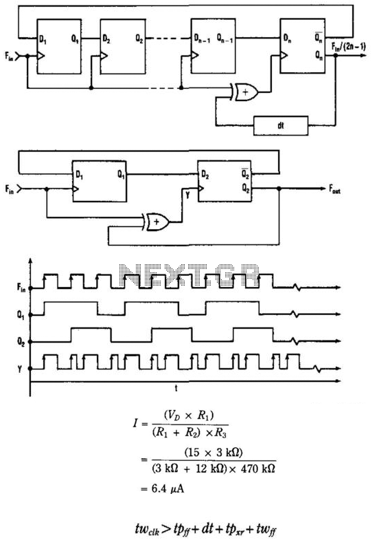
The described circuit is a frequency divider utilizing clocked flip-flops and an exclusive-OR gate to achieve a division of the input clock frequency. The division factor is determined by the formula 2^(n-1), where 'n' represents the number of flip-flops used in the circuit. The exclusive-OR gate plays a crucial role in feedback, ensuring that the output remains synchronized with the input clock.
The timing characteristics of the circuit are essential for its operation. The circuit's design allows for a negligible delay time, which is beneficial for high-frequency applications. The division by three is specifically highlighted, indicating that the circuit can produce an output frequency that is one-third of the input frequency. The steady-state output voltage of +13 V from the ICD is critical for the operation of the ICC, which further processes the signal.
Diodes D1 and D2 serve as critical components for controlling the flow of current and voltage levels within the circuit. D2 ensures that the voltage from the ICD is appropriately directed to the ICC, while D1 prevents backflow, allowing capacitor C1 to charge effectively. The charging of capacitor C1 is vital for maintaining the voltage levels necessary for the circuit's operation.
The inequality provided, t_wdk > t_Pff + dt + t_Pxr + t_Wff, establishes the timing requirements for the circuit. It indicates that the pulse width of the input clock must be sufficiently long to accommodate the delays introduced by the flip-flops and the exclusive-OR gate. The circuit's ability to operate at frequencies up to 22.5 MHz with standard 74F-type components demonstrates its robustness and efficiency in handling high-speed signals.
Overall, this frequency divider circuit is designed to produce an output signal that mirrors the duty cycle of the input clock, making it suitable for various applications in digital electronics where frequency division is required. 1. THE INPUT CLOCK frequency fed into this circuit is divided by 2n-l. The circuit consists of clocked flip- flops and one exclusive-OR gate. The dt delay is zero in most cases. 2. THIS CIRCUIT CONFIGURATION divides the input frequency by three (a). The circuit"s timing diagram verifies the division (b). The input signal drives ICD. Because ICD"s positive input (V + ) is slightly offset to +0.1 V, its steady-state output will be near +13 V. This voltage is sent to ICC through D2, setting ICC"s output to +13 V. Therefore, point D is cut off by Dl, and CI is charged by the current source. Assuming the initial voltage on CI is zero, the maximum voltage (i7Cmnx) is given by: twdk > tPff+ dt+ tpxr+ tWff The right side of the inequality should be the minimum pulse width (either up time or down time) of the input clock.
The circuit, when constructed with standard 74F-type parts, operates without any added delay in the exclusive-OR feedback path and with an input frequency of up to 22.5 MHz. The circuit"s output signal will have the same duty cycle as the input clock. 🔗 External reference
Related Circuits

A project is underway that necessitates the conversion of a 0-10V DC supply into a linear frequency range in the form of a square wave. The project involves designing a circuit that takes a direct current (DC) voltage input ranging...
This variable-frequency audio bandpass filter is constructed using two 741 operational amplifiers connected in cascade. The two 741 op amps are configured as identical RC active filters and are cascaded to enhance selectivity. The filter's tuning range spans from...
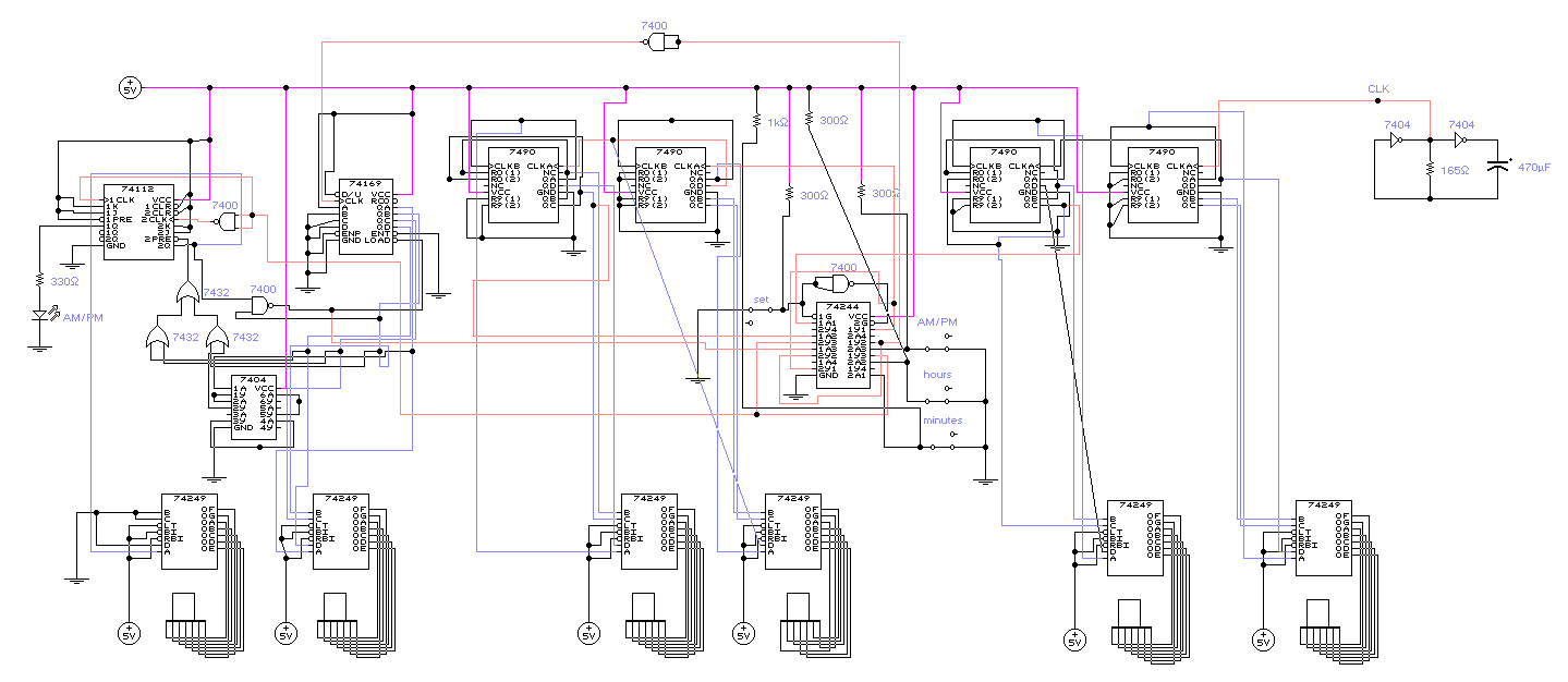
The 7490 counter is a negative edge-triggered decade counter that counts from 0 to 9. Pins CLKB and QA must be connected for this counter to operate in decade mode. The asynchronous reset pins R0(1, 2) and R9(1, 2)...
Comparing the performance of 1200V silicon carbide (SiC) MOSFETs with 1200V silicon MOSFETs and IGBTs at high frequency is essential to identify the differences in device losses and power-handling capabilities among these technologies. A demonstration platform has been developed...
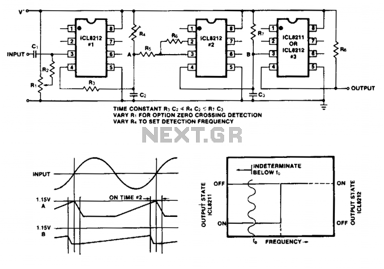
Simple frequency limit detectors providing a GO/NO-GO output for use with varying amplitude input signals may be conveniently implemented with the ICL8211/8212. In the application shown, the first ICL8212 is used as a zero-crossing detector. The output circuit consisting...
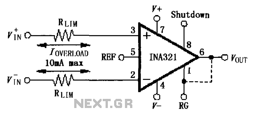
The input current protection circuit for the INA321/322 is illustrated. The INA321/322 features input terminal electrostatic discharge (ESD) protection diodes that become conductive when the input voltage exceeds the supply voltage by 500mV. The protection diodes will conduct, and...
Warning: include(partials/cookie-banner.php): Failed to open stream: Permission denied in /var/www/html/nextgr/view-circuit.php on line 713
Warning: include(): Failed opening 'partials/cookie-banner.php' for inclusion (include_path='.:/usr/share/php') in /var/www/html/nextgr/view-circuit.php on line 713