
Cmos-oscillator
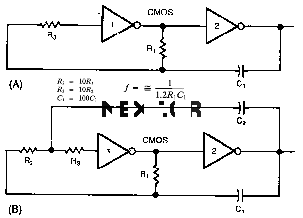
The common clock oscillator illustrated in Fig. 68-19A has two minor issues: it may not oscillate if the transition regions of its two gates differ. If it does oscillate, it might occasionally operate at a slightly lower frequency than predicted by its equation due to the finite gain of the first gate. When the circuit functions, oscillation typically occurs because both gates are housed in the same package, resulting in logic thresholds that are only a few millivolts apart. The circuit shown in Fig. 68-19B addresses both issues by incorporating a resistor and a capacitor. The R2/C2 network provides hysteresis, which delays the transition of gate 1 until C1 has sufficient voltage to securely move gate 1 through its transition region. Once gate 1 is in its transition region, C2 supplies positive feedback, rapidly moving gate 1 out of its transition region.
The common clock oscillator circuit is designed to generate a stable clock signal, which is crucial in various digital applications. The issues identified in the initial design stem from the characteristics of the gates used in the oscillator. The potential for the oscillator to fail to initiate oscillation arises from discrepancies in the transition regions of the gates, which can lead to unreliable performance. Additionally, the finite gain of the first gate can result in oscillation frequencies that deviate from theoretical predictions.
The solution proposed in Fig. 68-19B introduces a feedback mechanism through the R2/C2 network. The resistor R2 and capacitor C2 work together to create hysteresis, which is a critical feature that enhances the stability of the oscillator. Hysteresis ensures that there is a defined voltage threshold that must be crossed before the gate transitions from one state to another. This prevents false triggering and ensures that the oscillator operates reliably.
When the voltage across capacitor C1 reaches a certain level, it triggers gate 1 to transition. The addition of capacitor C2 is significant; it provides a positive feedback loop that accelerates the transition of gate 1 once it begins to change state. This rapid movement through the transition region minimizes the time spent in a state where the output is indeterminate, thus promoting a clean and stable oscillation.
Overall, the modifications introduced in Fig. 68-19B not only resolve the original issues of oscillation failure and frequency deviation but also enhance the overall performance and reliability of the clock oscillator circuit. This makes it suitable for various applications requiring precise timing signals.The common clock oscillator in Fig. 68-19A has two small problems: It might not, in fact, oscillate if the transition regions of its two gates differ. If it does oscillate, it might sometimes oscillate at a slightly lower frequency than its equation predicts because of the finite gain of the first gate.
If the circuit does work, oscillation occurs usually because both gates are in the package and, therefore, have logic thresholds only a few millivolts apart. The circuit in Fig. 68-19B resolves both problems by adding a resistor and a capacitor. The R2/ C2 network provides hysteresis, thus delaying the onset of gate 1 "s transition until Cl has enough voltage to move gate 1 securely through its transition region. When gate 1 is finally in its transition region, C2 provides positive feedback, thus rapidly moving gate 1 out of its transition region.
🔗 External reference
Related Circuits

This circuit is guaranteed to oscillate at a frequency of approximately 2.2/(R1 x C) if R2 is greater than R1. Additionally, the number of gates can be reduced further by replacing gates 1 and 2 with a non-inverting gate. The...
Warning: include(partials/cookie-banner.php): Failed to open stream: Permission denied in /var/www/html/nextgr/view-circuit.php on line 713
Warning: include(): Failed opening 'partials/cookie-banner.php' for inclusion (include_path='.:/usr/share/php') in /var/www/html/nextgr/view-circuit.php on line 713