
Coin Toss Circuit
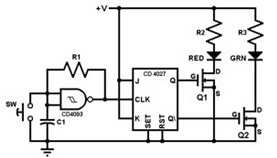
The coin toss circuit is designed to simulate a random selection process through the use of a square-wave oscillator and a JK flip-flop. The square-wave oscillator, implemented with a NAND gate from the CD4093, generates a continuous signal that toggles between high and low states. The frequency of this oscillation can be adjusted by changing the resistor (R1) and capacitor (C1) values; for instance, using a 100kΩ resistor and a 0.01µF capacitor yields a period of approximately 1ms, while a 0.001µF capacitor can achieve a faster oscillation of 0.1ms. This rapid toggling is essential for creating a visually dynamic indication through the LEDs.
The JK flip-flop, constructed using the CD4027 IC, takes the output from the oscillator as its clock input. The flip-flop's Q output will change state based on the clock signal, driving the LEDs. The connections to the flip-flop's pins are critical: pins 1 and 2 serve as the Q and Q' outputs, while pin 3 functions as the clock input. The reset (RST) and set (SET) pins are grounded, and the J and K inputs are tied to the positive supply voltage. This configuration allows the flip-flop to toggle its output with each clock pulse, resulting in one LED lighting up while the other turns off, thus simulating the randomness of a coin toss.
Proper assembly is crucial for the circuit's functionality. IC sockets should be used to facilitate easy replacement of the ICs if needed. The circuit board must be prepared with precise connections, ensuring that the battery clip wires are correctly soldered to the designated copper strips for power distribution. The switch must also be connected properly, as any misalignment can disrupt the circuit's operation. After assembly, a thorough inspection with an ohmmeter is recommended to check for shorts or incorrect connections before powering the circuit with a 9V battery.
Once powered, the circuit should exhibit the expected behavior: both LEDs light up initially, and pressing the switch will randomly toggle the states of the LEDs. This project serves as an excellent introduction to digital electronics, illustrating the principles of oscillation, state changes in flip-flops, and the use of basic components to create a functional electronic device.In this project you will build a coin toss circuit. It has three sections: a square-wave oscillator, a JK flip flop, and two LEDs (red & green). It uses CMOS digital ICs and MOSFET transistors. The schematic does not show the power and ground connections for the ICs. When powered from a 9V battery, both LEDs will light. When you press the switch, one LED shuts off and the other stays lit; but which one There`s a 50-50 chance for either color. The square-wave oscillator uses one gate in the CD4093 IC. The IC contains four 2-input NAND gates as shown in figure 2. Digital signals are either high (+V) or low (0V). The output of a gate will switch between high and low depending on its inputs. The input-output behavior of a gate is defined by its truth-table. Table 1 is the truth-table for a 2-input NAND gate where A and B are the inputs and X is the output. A 0 represents low (0V) while a 1 represents high (+V). Mistakes happen, and unsoldering an IC is tedious. So in this project we will use IC sockets. Refer to figure 6 to see how the parts are arranged on the board, including jumper wires. Figure 7 shows how the parts and jumpers are soldered. Note that the leads of the switch need to be adjusted slightly to fit the holes in the board. Figure 7 shows the two strips of copper that run along the top and bottom of the board. They are used for +9V (red wire on battery clip) and ground (black wire). Drill a 1/8 inch hole between the two existing holes. Then feed the battery clip wires through and make a small knot. Then feed the black and red wires through the other two holes as shown. In figure 6 you can see the red and black wires inserted into holes and soldered on the copper side. Note the bare-wire jumpers, including the one between the two ICs which brings +9V to pins 5 & 6 of the CD4027. Since I cut the board down, it turned out that the switch was connected to the same strips of copper as pins 4 and 7 of the CD4093.
So I had to cut two of the copper traces to isolate the switch from those pins. Be careful to insert the switch correctly. Use an ohmmeter to identify the normally open contacts. On the CD4093, input pins 1 & 2 and output pin 3 are used for the oscillator; pin 7 is ground and pin 14 is +9V. On the CD4027, pins 1 & 2 are used for Q & Q; pin 3 is the input (CLK); pins 4 & 7 (RST & SET) are connected to ground; pins 5 & 6 (K & J) are connected to +9V.
Pin 8 is ground and pin 16 is +9V. The exact values of R1 and C1 are not critical. I used 100k © and 0. 01 µF to get T = 1ms. Using 0. 001 µF for T = 0. 1ms would also work. Feel free to play around with values, but if the time constant gets too big, the LEDs will blink instead of being on steadily. Insert the ICs into their sockets; be careful to not put them in the wrong way. (You may have to squeeze both sides of an IC to get the pins to go into the socket. ) Before applying power, use an ohmmeter to verify there are no shorts between +9V and ground. Verify that the transistors and LEDs are in the right way. Verify that the jumpers connect to the correct points. Look for bad solder joints, missing solder joints, and shorted solder points. Verify that the red and black wires of the battery connector are soldered to the right places. If it passes final inspection, connect a 9V battery. The two LEDs should immediately light. Press the switch and verify one LED is off and the other is on. Repeat the process several times to verify that the color of the lit LED is red or green at random. 🔗 External reference
Related Circuits

This example describes the use of HS101 and HS201 radio transmitter and receiver modules to control rotating color lights, functioning as a multi-channel radio remote control device suitable for small dance floors or home use. Users positioned at any...
Detects the amount of salt contained in liquid foods, featuring a three-level LED indicator. This circuit is designed to detect the approximate percentage of salt concentration. The salt detection circuit operates by utilizing a conductivity sensor that measures the ionic...
A quad 2-input NAND Schmitt trigger circuit can be designed using the MC14093 CMOS type IC, which serves as a simple pulse width modulation (PWM) controller electronic project. This PWM controller is straightforward and requires only a few external...
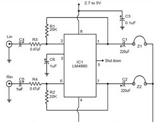
The LM4880 is a dual audio HiFi amplifier integrated circuit from National Semiconductor. This headphone amplifier circuit is specifically designed to produce high-quality audio output with a minimal number of components. The LM4880 integrated circuit is capable of delivering...

The RF2132 linear power amplifier circuit is depicted in the provided figure. A radio frequency (RF) signal enters through input pin 3 and is processed via a preamplifier. The final stage of the amplifier outputs a gain of 10....

Depending on the external circuit connection, the 555 timer can be configured for various modes such as start delay, trigger delay, multi-harmonic oscillation, and other operational conditions. It functions as a versatile tester with the inclusion of some RC...